ZHCSEY6E March   2013  – January 2023 DRV2667

PRODUCTION DATA  

  1. 特性
  2. 应用
  3. 说明
  4. Revision History
  5. Pin Configuration and Functions
  6. Specifications
    1. 6.1 Absolute Maximum Ratings
    2. 6.2 ESD Ratings
    3. 6.3 Recommended Operating Conditions
    4. 6.4 Thermal Information
    5. 6.5 Electrical Characteristics
    6. 6.6 Timing Requirements
    7. 6.7 Switching Characteristics
    8. 6.8 Typical Characteristics
  7. Detailed Description
    1. 7.1 Overview
    2. 7.2 Functional Block Diagram
    3. 7.3 Feature Description
      1. 7.3.1  Support for Haptic Piezo Actuators
      2. 7.3.2  Flexible Front End Interface
      3. 7.3.3  Ramp Down Behavior
      4. 7.3.4  Low Latency Startup
      5. 7.3.5  Low Power Standby Mode
      6. 7.3.6  Device Reset
      7. 7.3.7  Amplifier Gain
      8. 7.3.8  Adjustable Boost Voltage
      9. 7.3.9  Adjustable Current Limit
      10. 7.3.10 Internal Charge Pump
      11. 7.3.11 Device Protection
        1. 7.3.11.1 Thermal Protection
        2. 7.3.11.2 Overcurrent Protection
        3. 7.3.11.3 Brownout Protection
    4. 7.4 Device Functional Modes
      1. 7.4.1 FIFO Mode
        1. 7.4.1.1 Waveform Timeout
      2. 7.4.2 Direct Playback from RAM Mode
      3. 7.4.3 Waveform Synthesis Playback Mode
      4. 7.4.4 Waveform Sequencer
      5. 7.4.5 Analog Playback Mode
      6. 7.4.6 Low Voltage Operation Mode
    5. 7.5 Programming
      1. 7.5.1 Programming the Boost Voltage
      2. 7.5.2 Programming the Boost Current Limit
      3. 7.5.3 Programming the RAM
        1. 7.5.3.1 Accessing the RAM
        2. 7.5.3.2 RAM Format
          1. 7.5.3.2.1 Programming the Waveform Sequencer
      4. 7.5.4 I2C Interface
        1. 7.5.4.1 General I2C Operation
        2. 7.5.4.2 Single-Byte and Multiple-Byte Transfers
        3. 7.5.4.3 Single-Byte Write
        4. 7.5.4.4 Multiple-Byte Write and Incremental Multiple-Byte Write
        5. 7.5.4.5 Single-Byte Read
        6. 7.5.4.6 Multiple-Byte Read
    6. 7.6 Register Map
      1. 7.6.1  Address: 0x00
      2. 7.6.2  Address: 0x01
      3. 7.6.3  Address: 0x02
      4. 7.6.4  Address: 0x03
      5. 7.6.5  Address: 0x04
      6. 7.6.6  Address: 0x05
      7. 7.6.7  Address: 0x06
      8. 7.6.8  Address: 0x07
      9. 7.6.9  Address: 0x08
      10. 7.6.10 Address: 0x09
      11. 7.6.11 Address: 0x0A
      12. 7.6.12 Address: 0x0B
      13. 7.6.13 Address: 0xFF
  8. Application and Implementation
    1. 8.1 Application Information
    2. 8.2 Typical Application
      1. 8.2.1 Design Requirements
      2. 8.2.2 Detailed Design Procedure
        1. 8.2.2.1 Inductor Selection
        2. 8.2.2.2 Piezo Actuator Selection
        3. 8.2.2.3 Boost Capacitor Selection
        4. 8.2.2.4 Bulk Capacitor Selection
      3. 8.2.3 Application Curves
    3. 8.3 Initialization Setup
      1. 8.3.1 Initialization Procedure
      2. 8.3.2 Typical Usage Examples
        1. 8.3.2.1 Single Click or Alert Example
        2. 8.3.2.2 Library Storage Example
  9. Power Supply Recommendations
  10. 10Layout
    1. 10.1 Layout Guidelines
    2. 10.2 Layout Example
  11. 11Device and Documentation Support
    1. 11.1 Receiving Notification of Documentation Updates
    2. 11.2 Community Resources
    3. 11.3 Trademarks
  12. 12Mechanical, Packaging, and Orderable Information

封装选项

机械数据 (封装 | 引脚)
散热焊盘机械数据 (封装 | 引脚)
订购信息

Accessing the RAM

To maintain compatibility with the majority of standard I2C controllers, the DRV2667 device uses 8-bit addressing. To access 2 kB of RAM, a paging system is employed. The page register is located at address 0xFF. There are 8 memory pages that make up the 2048 bytes with 256 bytes on each page. Note that page 0 is reserved for register control space, as shown in Figure 7-4.
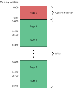
GUID-15DF2A7E-513B-4536-9BBC-AAE1EFFC13FD-low.gifFigure 7-4 Page Structure

Because the device addresses are only 8-bits, a special exception exists to distinguish whether the user is trying to write the page register at address 0xFF or the memory location at 0xPFF, where P represents the page number. In order to access the page register, the programmer must use a Single-Byte I2C protocol to perform a single-byte write to memory location 0xFF (see Section 7.5.4.3). To access the memory location in RAM at register 0xFF, the user must use the Incremental Multiple-Byte protocol (see Section 7.5.4.4), and the beginning address must be less than 0xFF.

The page register automatically increments for multiple-byte writes that cross the page boundaries, as a convenience for filling memory across multiple pages. Multiple-byte reads across page boundaries are not supported. All memory is retained in the device until the device power is cycled.