ZHCSDG6C March 2015 – January 2023 DRV2700
PRODUCTION DATA
- 1 特性
- 2 应用
- 3 说明
- 4 Revision History
- 5 Pin Configuration and Functions
- 6 Specifications
- 7 Detailed Description
-
8 Application and Implementation
- 8.1 Application Information
- 8.2
Typical Applications
- 8.2.1
AC-Coupled DAC Input Application
- 8.2.1.1 Design Requirements
- 8.2.1.2
Detailed Design Procedure
- 8.2.1.2.1 Piezo Load Selection
- 8.2.1.2.2 Programming The Boost Voltage
- 8.2.1.2.3 Inductor and Transformer Selection
- 8.2.1.2.4 Programing the Boost and Flyback Current-Limit
- 8.2.1.2.5 Boost Capacitor Selection
- 8.2.1.2.6 Pulldown FET and Resistors
- 8.2.1.2.7 Low-Voltage Operation
- 8.2.1.2.8 Current Consumption Calculation
- 8.2.1.2.9 Input Filter Considerations
- 8.2.1.2.10 Output Limiting Factors
- 8.2.1.2.11 Startup and Shutdown Sequencing
- 8.2.1.3 Application Curves
- 8.2.2 Filtered AC Coupled Single-Ended PWM Input Application
- 8.2.3 DC-Coupled DAC Input Application
- 8.2.4 DC-Coupled Reference Input Application
- 8.2.5 Flyback Circuit
- 8.2.1
AC-Coupled DAC Input Application
- 8.3 System Example
- 9 Power Supply Recommendations
- 10Layout
- 11Device and Documentation Support
- 12Mechanical, Packaging, and Orderable Information
5 Pin Configuration and Functions

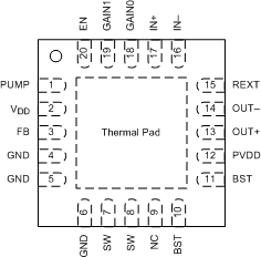
NC – no internal connection
Figure 5-1 RGP Package20-Pin VQFN With Exposed Thermal Pad Top ViewPin Functions
| PIN | TYPE(1) | CONNECTION IF UNUSED | DESCRIPTION | |
|---|---|---|---|---|
| NAME | NO. | |||
| BST | 10 | P | — | Boost output voltage |
| 11 | — | |||
| EN | 20 | I | — | Chip enable |
| FB | 3 | I | — | Boost feedback |
| GAIN0 | 18 | I | GND | Gain programming pin — least significant bit (LSB) |
| GAIN1 | 19 | I | GND | Gain programming pin — most significant bit (MSB) |
| GND | 4 | P | — | Ground |
| 5 | — | |||
| 6 | — | |||
| IN+ | 17 | I | NC | Noninverting input |
| IN– | 16 | I | NC | Inverting input |
| NC | 9 | — | — | No connect |
| OUT+ | 13 | O | NC | Noninverting output |
| OUT– | 14 | O | NC | Inverting output |
| PVDD | 12 | P | NC | Amplifier supply voltage |
| PUMP | 1 | P | — | Internal charge-pump voltage |
| REXT | 15 | I | — | Resistor to ground. This pin sets the boost current-limit. |
| SW | 7 | P | — | Internal-boost switch pin |
| 8 | — | |||
| VDD | 2 | P | — | Power supply (connect to battery) |
(1) I = Input, O = Output, I/O = Input and output, P = Power