ZHCSHJ5 December   2018 DRV5021

PRODUCTION DATA.  

  1. 特性
  2. 应用
  3. 说明
    1.     Device Images
      1.      典型应用电路原理图
      2.      磁响应
  4. 修订历史记录
  5. Pin Configuration and Functions
    1.     Pin Functions
  6. Specifications
    1. 6.1 Absolute Maximum Ratings
    2. 6.2 ESD Ratings
    3. 6.3 Recommended Operating Conditions
    4. 6.4 Thermal Information
    5. 6.5 Electrical Characteristics
    6. 6.6 Magnetic Characteristics
    7. 6.7 Typical Characteristics
  7. Detailed Description
    1. 7.1 Overview
    2. 7.2 Functional Block Diagram
    3. 7.3 Feature Description
      1. 7.3.1 Field Direction Definition
      2. 7.3.2 Device Output
      3. 7.3.3 Power-On Time
      4. 7.3.4 Hall Element Location
      5. 7.3.5 Propagation Delay
      6. 7.3.6 Output Stage
    4. 7.4 Device Functional Modes
  8. Application and Implementation
    1. 8.1 Application Information
    2. 8.2 Typical Applications
      1. 8.2.1 Proximity Sensing Circuit
        1. 8.2.1.1 Design Requirements
        2. 8.2.1.2 Detailed Design Procedure
          1. 8.2.1.2.1 Configuration Example
        3. 8.2.1.3 Application Curves
      2. 8.2.2 Alternative Two-Wire Application
        1. 8.2.2.1 Design Requirements
        2. 8.2.2.2 Detailed Design Procedure
  9. Power Supply Recommendations
  10. 10Layout
    1. 10.1 Layout Guidelines
    2. 10.2 Layout Example
  11. 11器件和文档支持
    1. 11.1 文档支持
      1. 11.1.1 相关文档
    2. 11.2 接收文档更新通知
    3. 11.3 社区资源
    4. 11.4 商标
    5. 11.5 静电放电警告
    6. 11.6 术语表
  12. 12机械、封装和可订购信息

封装选项

机械数据 (封装 | 引脚)
散热焊盘机械数据 (封装 | 引脚)
订购信息

Power-On Time

After applying VCC to the DRV5021, ton must elapse before the OUT pin is valid. In case 1 (Figure 13) and case 2 (Figure 14), the output is defined assuming that magnetic field BAPPLIED > BOP, and BAPPLIED < BRP, respectively.
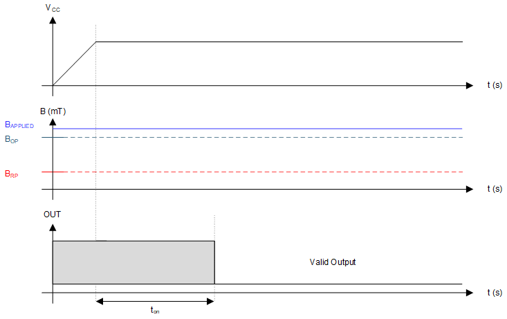
DRV5021 drv5021_timing_case1.gifFigure 13. Case 1: Power On When B > BOP
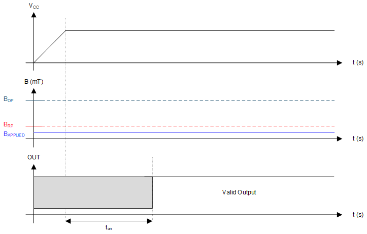
DRV5021 drv5021_timing_case2.gifFigure 14. Case 2: Power On When B < BRP

If the device is powered on with BRP < BAPPLIED < BOP, then the device output remains in indeterminate state until the magnetic field changes. After the change in magnetic field results in a condition that meets either BOP < BAPPLIED or BRP > BAPPLIED, the output turns to valid state after td time elapses. Case 3 (Figure 15) and case 4 (Figure 16) show examples of this behavior.
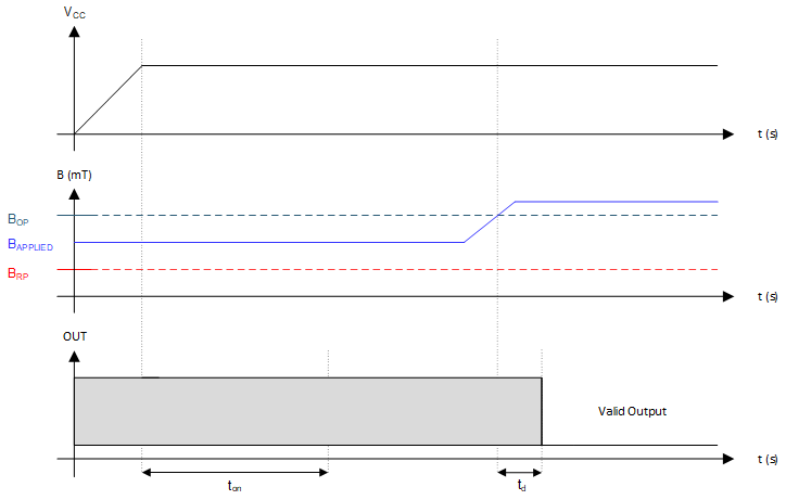
DRV5021 drv5021_timing_case3.gifFigure 15. Case 3: Power On When BRP < B < BOP, Followed by B > BOP
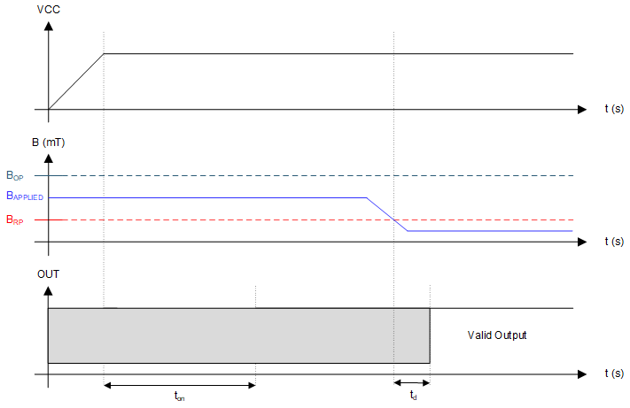
DRV5021 drv5021_timing_case4.gifFigure 16. Case 4: Power On When BRP < B < BOP, Followed by B < BRP