ZHCSEF4G December 2014 – March 2017 DRV5023-Q1
PRODUCTION DATA.
7 Detailed Description
7.1 Overview
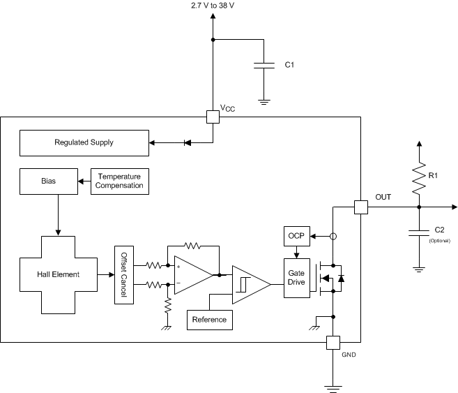
The DRV5023-Q1 device is a chopper-stabilized Hall sensor with a digital output for magnetic sensing applications. The DRV5023-Q1 device can be powered with a supply voltage between 2.7 and 38 V, and will survive –22 V reverse-battery conditions. The DRV5023-Q1 device does not operate when –22 to 2.4 V is applied to the VCC pin (with respect to GND pin). In addition, the device can withstand supply voltages up to 40 V for transient durations.
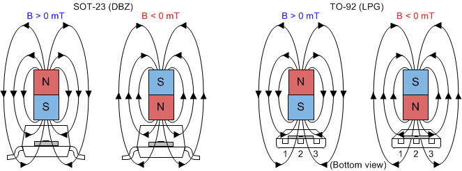
The field polarity is defined as follows: a south pole near the marked side of the package is a positive magnetic field. A north pole near the marked side of the package is a negative magnetic field. The output state is dependent on the magnetic field perpendicular to the package.
For the FA, AJ, and BI device versions, a strong south pole near the marked side of the package causes the output to pull low, and the absence of a field makes the output high-impedance. The FI version has an inverted output response, where a strong south pole causes the output to be high-impedance, and the absence of a field makes the output pull low. Hysteresis is included in between the operate point and the release point to prevent toggling near the magnetic threshold.
An external pullup resistor is required on the OUT pin. The OUT pin can be pulled up to VCC, or to a different voltage supply. This allows for easier interfacing with controller circuits.
7.2 Functional Block Diagram
7.3 Feature Description
7.3.1 Field Direction Definition
A positive magnetic field is defined as a south pole near the marked side of the package as shown in Figure 11.
7.3.2 Device Output
If the device is powered on with a magnetic field strength between BRP and BOP, then the device output is indeterminate and can either be Hi-Z or Low. For the FA, AJ, and BI device versions, if the field strength is greater than BOP, then the output is pulled low; if the field strength is less than BRP, then the output is released. For the FI device version, if the field strength is greater than BOP, then the output is Hi-Z; if the field strength is less than BRP, then the output is pulled Low.
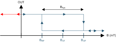 Figure 12. Output State of FA, AJ, BI Versions
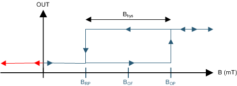 Figure 13. Output State of FI Version
7.3.3 Power-On Time
After applying VCC to the DRV5023-Q1 device, ton must elapse before the OUT pin is valid. During the power-up sequence, the output is Hi-Z. A pulse as shown in Figure 14 and Figure 15 occurs at the end of ton. This pulse can allow the host processor to determine when the DRV5023-Q1 output is valid after startup. In Case 1 (Figure 14) and Case 2 (Figure 15), the output is defined assuming a constant magnetic field B > BOP and B < BRP.
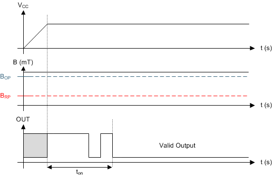 Figure 14. Case 1: Power On When B > BOP
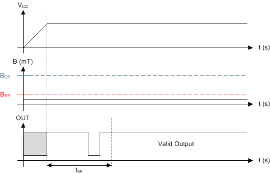 Figure 15. Case 2: Power On When B < BRP
If the device is powered on with the magnetic field strength BRP < B < BOP, then the device output is indeterminate and can either be Hi-Z or pulled low. During the power-up sequence, the output is held Hi-Z until ton has elapsed. At the end of ton, a pulse is given on the OUT pin to indicate that ton has elapsed. After ton, if the magnetic field changes such that BOP < B, the output is released. Case 3 (Figure 16) and Case 4 (Figure 17) show examples of this behavior.
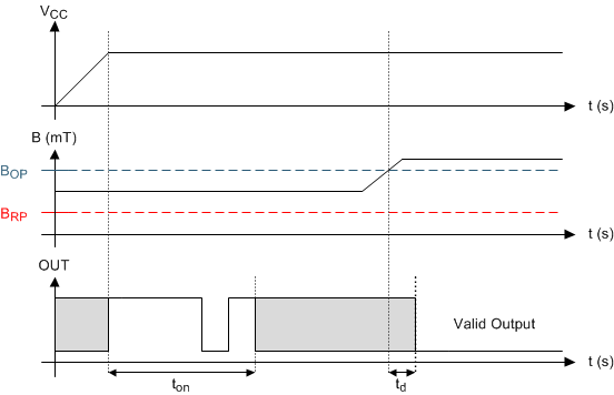 Figure 16. Case 3: Power On When BRP < B < BOP, Followed by B > BOP
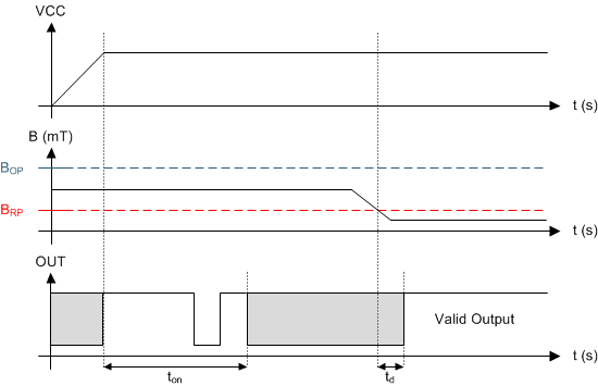 Figure 17. Case 4: Power On When BRP < B < BOP, Followed by B < BRP
7.3.4 Output Stage
The DRV5023-Q1 output stage uses an open-drain NMOS, and it is rated to sink up to 30 mA of current. For proper operation, calculate the value of the pullup resistor R1 using Equation 1.

The size of R1 is a tradeoff between the OUT rise time and the current when OUT is pulled low. A lower current is generally better, however faster transitions and bandwidth require a smaller resistor for faster switching.
In addition, ensure that the value of R1 > 500 Ω to ensure the output driver can pull the OUT pin close to GND.
NOTE
Vref is not restricted to VCC. The allowable voltage range of this pin is specified in the Absolute Maximum Ratings.
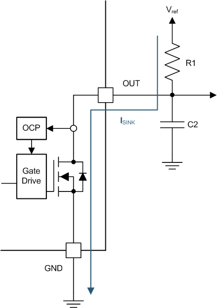 Figure 18.
Select a value for C2 based on the system bandwidth specifications as shown in Equation 2.

Most applications do not require this C2 filtering capacitor.
7.3.5 Protection Circuits
The DRV5023-Q1 device is fully protected against overcurrent and reverse-supply conditions.
7.3.5.1 Overcurrent Protection (OCP)
An analog current-limit circuit limits the current through the FET. The driver current is clamped to IOCP. During this clamping, the rDS(on) of the output FET is increased from the nominal value.
7.3.5.2 Load Dump Protection
The DRV5023-Q1 device operates at DC VCC conditions up to 38 V nominally, and can additionally withstand VCC = 40 V. No current-limiting series resistor is required for this protection.
7.3.5.3 Reverse Supply Protection
The DRV5023-Q1 device is protected in the event that the VCC pin and the GND pin are reversed (up to –22 V).
NOTE
In a reverse supply condition, the OUT pin reverse-current must not exceed the ratings specified in the Absolute Maximum Ratings.
Table 1.
| FAULT | CONDITION | DEVICE | DESCRIPTION | RECOVERY |
|---|---|---|---|---|
| FET overload (OCP) | ISINK ≥ IOCP | Operating | Output current is clamped to IOCP | IO < IOCP |
| Load dump | 38 V < VCC < 40 V | Operating | Device will operate for a transient duration | VCC ≤ 38 V |
| Reverse supply | –22 V < VCC < 0 V | Disabled | Device will survive this condition | VCC ≥ 2.7 V |
7.3.5.4 Output Jitter Characteristic
The DRV5023-Q1 propagation delay is not fully consistent. If a periodic magnetic field is applied, the device introduces a small amount of jitter on the output. The tj parameter describes this characteristic and Figure 19 shows the test waveform.
 Figure 19. Test Waveform for tj
7.4 Device Functional Modes
The DRV5023-Q1 device is active only when VCC is between 2.7 and 38 V.
When a reverse supply condition exists, the device is inactive.