-
DRV5033 数字全极开关霍尔效应传感器
DATA SHEET
DRV5033 数字全极开关霍尔效应传感器
本资源的原文使用英文撰写。 为方便起见,TI 提供了译文;由于翻译过程中可能使用了自动化工具,TI 不保证译文的准确性。 为确认准确性,请务必访问 ti.com 参考最新的英文版本(控制文档)。
1 特性
- 数字全极开关霍尔传感器
- 出色的温度稳定性
- 在温度范围内 BOP ±10%
- 多种灵敏度选项 (BOP/BRP):
- 检测南北磁场
- 支持宽电压范围
- 2.5V 至 38V
- 无需外部稳压器
- 宽运行电压范围
- TA = -40 至 125°C(Q,请见 Figure 24)
- 开漏输出(30mA 灌电流)
- 35µs 快速上电时间
- 小型封装尺寸
- 表面贴装 3 引脚小外形尺寸晶体管 (SOT)-23 (DBZ)
- 2.92mm × 2.37mm
- 插入式 3 引脚 TO-92 (LPG)
- 4.00mm × 3.15mm
- 表面贴装 3 引脚小外形尺寸晶体管 (SOT)-23 (DBZ)
-
保护 特性
- 反向电源保护(高达 -22V)
- 支持高达 40V 抛负载
- 输出短路保护
- 输出电流限制
2 应用
- 对接检测
- 门开关检测
- 接近感测
- 阀定位
- 脉冲计数
3 说明
DRV5033 器件是一款斩波稳定霍尔效应传感器,能够在整个温度范围内提供具有出色灵敏度稳定性和集成保护特性的磁场感测 功能。
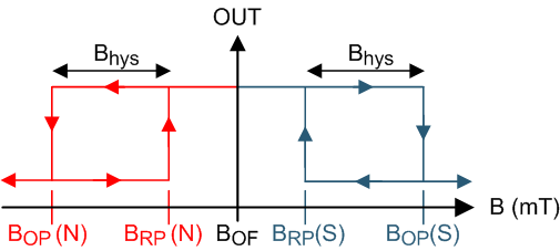
DRV5033 对磁场两极方向的响应相同。当应用的磁通量密度超过 BOP 阈值时,DRV5033 开漏输出变为低电平。输出将保持低电平,直到磁通量密度降至 BRP 以下之后变为高阻抗。输出灌电流能力为 30mA。反向极性保护高达 -22V 的宽工作电压范围(2.5 至 38V)使得此器件广泛适用于各种工业 信号。
该器件提供针对反向电源情况、负载突降以及输出短路或过流故障的内部保护功能。
器件信息(1)
| 器件型号 | 封装 | 封装尺寸(标称值) |
|---|---|---|
| DRV5033 | SOT-23 (3) | 2.92mm × 1.30mm |
| TO-92 (3) | 4.00mm × 3.15mm |
- 要了解所有可用封装,请见数据表末尾的可订购米6体育平台手机版_好二三四附录。
输出状态
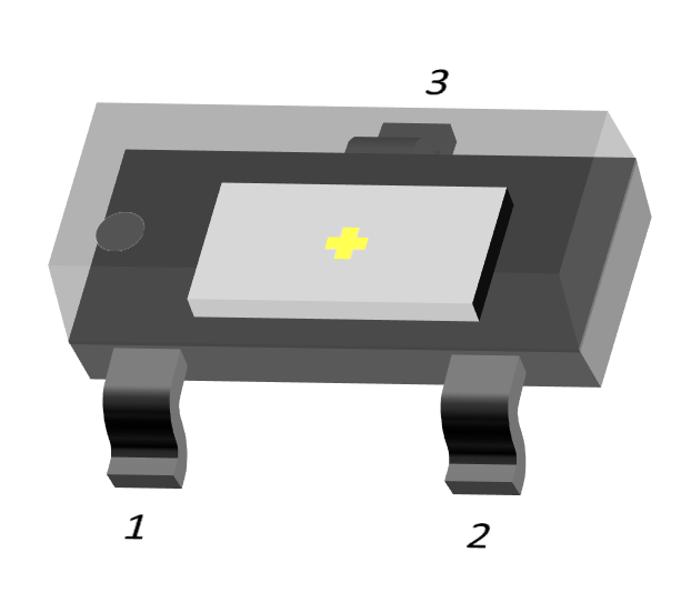
SOT-23
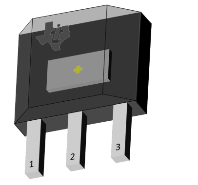
TO-92
4 修订历史记录
Changes from F Revision (May 2016) to G Revision
- Changed the power-on time for the FA version in the Electrical Characteristics tableGo
- Added the Layout section Go
- Added 接收文档更新通知部分Go
Changes from E Revision (February 2016) to F Revision
- Revised preliminary limits for the FA versionGo
Changes from D Revision (December 2015) to E Revision
Changes from C Revision (May 2015) to D Revision
- 已更正 SOT-23 封装体尺寸并将 SIP 封装名称更正为 TO-92 Go
- Added BMAX to Absolute Maximum Ratings Go
- Removed table note from junction temperature Go
- 已更新封装卷带选项 M 和空白Go
- 已添加 社区资源 Go
Changes from B Revision (September 2014) to C Revision
- 已将器件状态更新为量产数据 Go
Changes from A Revision (August 2014) to B Revision
- Changed the maximum TJ value to 150°C Go
- Added typical rise and fall time and removed maximum value in Switching Characteristics Go
- Updated the Magnetic Characteristics values Go
- Updated all Typical Characteristics graphs Go
- Updated Equation 4 Go
Changes from * Revision (May 2014) to A Revision
5 Pin Configuration and Functions
For additional configuration information, see 器件标记 and 机械、封装和可订购信息.
DBZ Package
3-Pin SOT-23
Top View
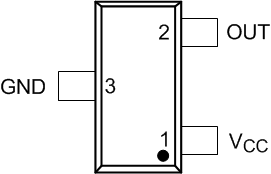
LPG Package
3-Pin TO-92
Top View

Pin Functions
| PIN | TYPE | DESCRIPTION | ||
|---|---|---|---|---|
| NAME | DBZ | LPG | ||
| GND | 3 | 2 | GND | Ground pin |
| OUT | 2 | 3 | Output | Hall sensor open-drain output. The open drain requires a resistor pullup. |
| VCC | 1 | 1 | PWR | 2.5 to 38 V power supply. Bypass this pin to the GND pin with a 0.01-µF (minimum) ceramic capacitor rated for VCC. |
6 Specifications
6.1 Absolute Maximum Ratings
over operating free-air temperature range (unless otherwise noted) (1)| MIN | MAX | UNIT | ||
|---|---|---|---|---|
| Power supply voltage | VCC | –22(2) | 40 | V |
| Voltage ramp rate (VCC), VCC < 5 V | Unlimited | V/µs | ||
| Voltage ramp rate (VCC), VCC > 5 V | 0 | 2 | ||
| Output pin voltage | –0.5 | 40 | V | |
| Output pin reverse current during reverse supply condition | 0 | 100 | mA | |
| Magnetic flux density, BMAX | Unlimited | |||
| Operating junction temperature, TJ | –40 | 150 | °C | |
| Storage temperature, Tstg | –65 | 150 | °C | |
(1) Stresses beyond those listed under Absolute Maximum Ratings may cause permanent damage to the device. These are stress ratings only, which do not imply functional operation of the device at these or any other conditions beyond those indicated under Recommended Operating Conditions. Exposure to absolute-maximum-rated conditions for extended periods may affect device reliability.
(2) Ensured by design. Only tested to –20 V.
6.2 ESD Ratings
| VALUE | UNIT | |||
|---|---|---|---|---|
| V(ESD) | Electrostatic discharge | Human body model (HBM), per ANSI/ESDA/JEDEC JS-001, all pins(1) | ±2500 | V |
| Charged device model (CDM), per JEDEC specification JESD22-C101, all pins(2) | ±500 | |||
(1) JEDEC document JEP155 states that 500-V HBM allows safe manufacturing with a standard ESD control process.
(2) JEDEC document JEP157 states that 250-V CDM allows safe manufacturing with a standard ESD control process.
6.3 Recommended Operating Conditions
over operating free-air temperature range (unless otherwise noted)| MIN | MAX | UNIT | |||
|---|---|---|---|---|---|
| VCC | Power supply voltage | 2.5 | 38 | V | |
| VO | Output pin voltage (OUT) | 0 | 38 | V | |
| ISINK | Output pin current sink (OUT)(1) | 0 | 30 | mA | |
| TA | Operating ambient temperature | –40 | 125 | °C | |
(1) Power dissipation and thermal limits must be observed
6.4 Thermal Information
| THERMAL METRIC(1) | DRV5033 | UNIT | ||
|---|---|---|---|---|
| DBZ (SOT-23) | LPG (TO-92) | |||
| 3 PINS | 3 PINS | |||
| RθJA | Junction-to-ambient thermal resistance | 333.2 | 180 | °C/W |
| RθJC(top) | Junction-to-case (top) thermal resistance | 99.9 | 98.6 | °C/W |
| RθJB | Junction-to-board thermal resistance | 66.9 | 154.9 | °C/W |
| ψJT | Junction-to-top characterization parameter | 4.9 | 40 | °C/W |
| ψJB | Junction-to-board characterization parameter | 65.2 | 154.9 | °C/W |
(1) For more information about traditional and new thermal metrics, see the Semiconductor and IC Package Thermal Metrics application report, SPRA953.
6.5 Electrical Characteristics
over operating free-air temperature range (unless otherwise noted)6.6 Switching Characteristics
over operating free-air temperature range (unless otherwise noted)6.7 Magnetic Characteristics
over operating free-air temperature range (unless otherwise noted)| PARAMETER | TEST CONDITIONS | MIN | TYP | MAX | UNIT(1) | |
|---|---|---|---|---|---|---|
| ƒBW | Bandwidth(2) | 20 | 30 | kHz | ||
| DRV5033FA: ±3.5 / ±2 mT | ||||||
| BOP | Operate point; see Figure 12 | TA = –40°C to 125°C | ±1.8 | ±3.5 | ±6.8 | mT |
| BRP | Release point; see Figure 12 | ±0.5 | ±2 | ±4.2 | mT | |
| Bhys | Hysteresis; Bhys = (BOP – BRP)(3) | ±1.5 | mT | |||
| BO | Magnetic offset; BO = (BOP + BRP) / 2 | ±2.8 | mT | |||
| DRV5033AJ: ±6.9 / ±3.5 mT | ||||||
| BOP | Operate point; see Figure 12 | TA = –40°C to 125°C | ±3 | ±6.9 | ±12 | mT |
| BRP | Release point; see Figure 12 | ±1 | ±3.5 | ±5 | mT | |
| Bhys | Hysteresis; Bhys = (BOP – BRP)(3) | 3.4 | mT | |||
| BO | Magnetic offset; BO = (BOP + BRP) / 2 | 5.2 | mT | |||
(1) 1 mT = 10 Gauss
(2) Bandwidth describes the fastest changing magnetic field that can be detected and translated to the output.
(3) |BOP| is always greater than |BRP|.
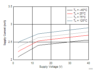
6.8 Typical Characteristics
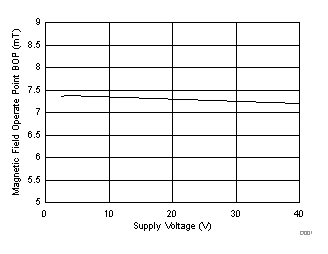
| TA = 25°C | ||
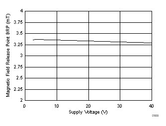
| TA = 25°C |
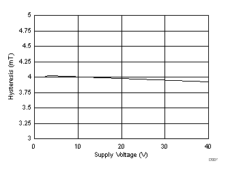
| TA = 25°C |
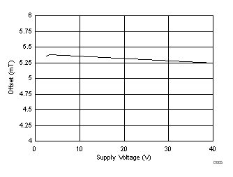
| TA = 25°C |
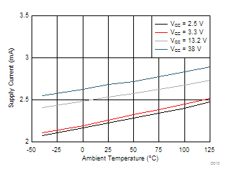
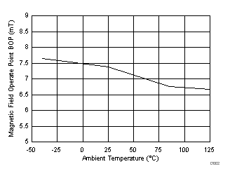
| VCC = 3.3 V | ||
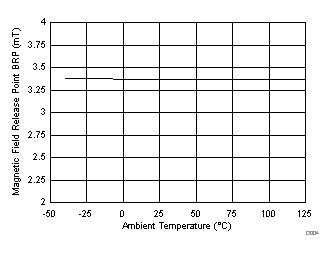
| VCC = 3.3 V |
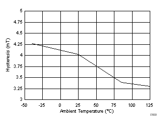
| VCC = 3.3 V |
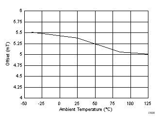
| VCC = 3.3 V |
