SLVSGC3 May   2020 DRV8210P

PRODUCTION DATA  

  1. Features
  2. Applications
  3. Description
  4. Revision History
  5. Device Comparison
  6. Pin Configuration and Functions
  7. Specifications
    1. 7.1 Absolute Maximum Ratings
    2. 7.2 ESD Ratings
    3. 7.3 Recommended Operating Conditions
    4. 7.4 Thermal Information
    5. 7.5 Electrical Characteristics
    6. 7.6 Typical Characteristics
  8. Detailed Description
    1. 8.1 Overview
    2. 8.2 Functional Block Diagram
    3. 8.3 Feature Description
      1. 8.3.1 External Components
      2. 8.3.2 Control Modes
        1. 8.3.2.1 PWM Control
      3. 8.3.3 Protection Circuits
        1. 8.3.3.1 Supply Undervoltage Lockout (UVLO)
        2. 8.3.3.2 OUTx Overcurrent Protection (OCP)
        3. 8.3.3.3 Thermal Shutdown (TSD)
      4. 8.3.4 Pin Diagrams
        1. 8.3.4.1 Logic-Level Inputs
    4. 8.4 Device Functional Modes
      1. 8.4.1 Active Mode
      2. 8.4.2 Low-Power Sleep Mode
      3. 8.4.3 Fault Mode
  9. Application and Implementation
    1. 9.1 Application Information
    2. 9.2 Typical Application
      1. 9.2.1 Full-Bridge Driving
        1. 9.2.1.1 Design Requirements
        2. 9.2.1.2 Detailed Design Procedure
          1. 9.2.1.2.1 Supply Voltage
          2. 9.2.1.2.2 Control Interface
          3. 9.2.1.2.3 Low-Power Operation
        3. 9.2.1.3 Application Curves
      2. 9.2.2 Dual-Coil Relay Driving
        1. 9.2.2.1 Design Requirements
        2. 9.2.2.2 Detailed Design Procedure
          1. 9.2.2.2.1 Supply Voltage
          2. 9.2.2.2.2 Control Interface
          3. 9.2.2.2.3 Low-Power Operation
        3. 9.2.2.3 Application Curves
      3. 9.2.3 Current Sense
        1. 9.2.3.1 Design Requirements
        2. 9.2.3.2 Detailed Design Procedure
          1. 9.2.3.2.1 Shunt Resistor Sizing
    3. 9.3 Current Capability and Thermal Performance
      1. 9.3.1 Power Dissipation and Output Current Capability
      2. 9.3.2 Thermal Performance
        1. 9.3.2.1 Steady-State Thermal Performance
        2. 9.3.2.2 Transient Thermal Performance
  10. 10Power Supply Recommendations
    1. 10.1 Bulk Capacitance
  11. 11Layout
    1. 11.1 Layout Guidelines
    2. 11.2 Layout Example
  12. 12Device and Documentation Support
    1. 12.1 Documentation Support
      1. 12.1.1 Related Documentation
    2. 12.2 Receiving Notification of Documentation Updates
    3. 12.3 Support Resources
    4. 12.4 Trademarks
    5. 12.5 Electrostatic Discharge Caution
    6. 12.6 Glossary
  13. 13Mechanical, Packaging, and Orderable Information

封装选项

机械数据 (封装 | 引脚)
散热焊盘机械数据 (封装 | 引脚)
订购信息

Pin Configuration and Functions

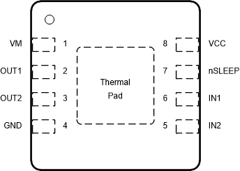
GUID-8B516976-0A25-455F-A306-D43662486F67-low.gif Figure 6-1 DRV8210P DSG Package8-Pin WSONTop View
Table 6-1 Pin Functions
PIN TYPE DESCRIPTION
NAME NO.
GND 4 PWR Device ground. Connect to system ground.
IN1 6 I H-bridge control input. See Section 8.3.2. Internal pulldown resistor.
IN2 5 I H-bridge control input. See Section 8.3.2. Internal pulldown resistor.
nSLEEP 7 I Sleep mode input. Set this pin to logic high to enable the device. Set this pin to logic low to go to low-power sleep mode. Internal pulldown resistor.
OUT1 2 O H-bridge output. Connect to the motor or other load.
OUT2 3 O H-bridge output. Connect to the motor or other load.
VM 1 PWR Motor power supply. Bypass this pin to the GND pin with a 0.1-µF ceramic capacitor as well as sufficient bulk capacitance rated for VM.
VCC 8 PWR Logic power supply. Bypass this pin to the GND pin with a 0.1-µF ceramic capacitor rated for VCC.
PAD Thermal pad. Connect to system ground.