ZHCSMP7 November 2021 DRV8231
PRODUCTION DATA
- 1 特性
- 2 应用
- 3 说明
- 4 Revision History
- 5 Device Comparison
- 6 Pin Configuration and Functions
- 7 Specifications
- 8 Detailed Description
- 9 Application and Implementation
- 10Power Supply Recommendations
- 11Layout
- 12Device and Documentation Support
- 13Mechanical, Packaging, and Orderable Information
封装选项
机械数据 (封装 | 引脚)
散热焊盘机械数据 (封装 | 引脚)
订购信息
8.4.1 Bridge Control
The DRV8231 output consists of four N-channel MOSFETs that are designed to drive high current. These outputs are controlled by the two logic inputs IN1 and IN2 as listed in Table 8-2.
| IN1 | IN2 | OUT1 | OUT2 | DESCRIPTION |
|---|---|---|---|---|
| 0 | 0 | High-Z | High-Z | Coast; H-bridge disabled to High-Z (sleep entered after 1 ms) |
| 0 | 1 | L | H | Reverse (Current OUT2 → OUT1) |
| 1 | 0 | H | L | Forward (Current OUT1 → OUT2) |
| 1 | 1 | L | L | Brake; low-side slow decay |
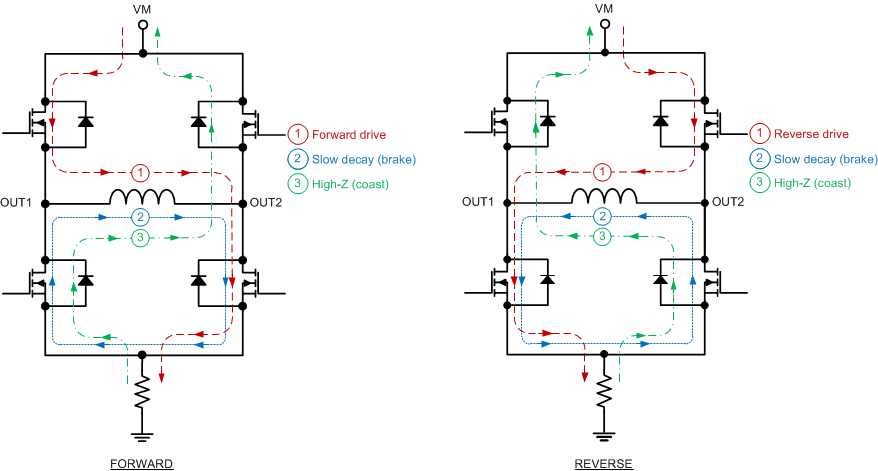
The inputs can be set to static voltages for 100% duty cycle drive, or they can be pulse-width modulated (PWM) for variable motor speed. When using PWM, switching between driving and braking typically works best. For example, to drive a motor forward with 50% of the maximum RPM, IN1 = 1 and IN2 = 0 during the driving period, and IN1 = 1 and IN2 = 1 during the other period. Alternatively, the coast mode (IN1 = 0, IN2 = 0) for fast current decay is also available. Figure 8-1 shows how the motor current flows through the H-bridge. The input pins can be powered before VM is applied.
 Figure 8-1 H-Bridge
Current Paths
Figure 8-1 H-Bridge
Current PathsWhen an output changes from driving high to driving low, or driving low to driving high, dead time is automatically inserted to prevent shoot-through. The tDEAD time is the time in the middle when the output is High-Z. If the output pin is measured during tDEAD, the voltage depends on the direction of current. If the current is leaving the pin, the voltage is a diode drop below ground. If the current is entering the pin, the voltage is a diode drop above VM. This diode is the body diode of the high-side or low-side FET.
The propagation delay time (tPD) is measured as the time between an input edge to output change. This time accounts for input deglitch time and other internal logic propagation delays. The input deglitch time prevents noise on the input pins from affecting the output state. Additional output slew delay timing accounts for FET turn on or turn off times (tRISE and tFALL).
Figure 8-2 below shows the timing of the inputs and outputs of the motor driver.