ZHCSPH2 January   2022 DRV8251A

PRODUCTION DATA  

  1. 特性
  2. 应用
  3. 说明
  4. Revision History
  5. Device Comparison
  6. Pin Configuration and Functions
  7. Specifications
    1. 7.1 Absolute Maximum Ratings
    2. 7.2 ESD Ratings
    3. 7.3 Recommended Operating Conditions
    4. 7.4 Thermal Information
    5. 7.5 Electrical Characteristics
    6. 7.6 Typical Characteristics
    7. 7.7 Timing Diagrams
  8. Detailed Description
    1. 8.1 Overview
    2. 8.2 Functional Block Diagram
    3. 8.3 External Components
    4. 8.4 Feature Description
      1. 8.4.1 Bridge Control
      2. 8.4.2 Current Sense and Regulation (IPROPI)
        1. 8.4.2.1 Current Sensing
        2. 8.4.2.2 Current Regulation
      3. 8.4.3 Protection Circuits
        1. 8.4.3.1 Overcurrent Protection (OCP)
        2. 8.4.3.2 Thermal Shutdown (TSD)
        3. 8.4.3.3 VM Undervoltage Lockout (UVLO)
    5. 8.5 Device Functional Modes
      1. 8.5.1 Active Mode
      2. 8.5.2 Low-Power Sleep Mode
      3. 8.5.3 Fault Mode
    6. 8.6 Pin Diagrams
      1. 8.6.1 Logic-Level Inputs
  9. Application and Implementation
    1. 9.1 Application Information
    2. 9.2 Typical Application
      1. 9.2.1 Brush DC Motor
        1. 9.2.1.1 Design Requirements
        2. 9.2.1.2 Detailed Design Procedure
          1. 9.2.1.2.1 Motor Voltage
          2. 9.2.1.2.2 Motor Current
        3. 9.2.1.3 Application Curves
      2. 9.2.2 Stall Detection
        1. 9.2.2.1 Design Requirements
        2. 9.2.2.2 Detailed Design Procedure
          1. 9.2.2.2.1 Stall Detection Timing
          2. 9.2.2.2.2 Stall Threshold Selection
        3. 9.2.2.3 Application Curves
      3. 9.2.3 Relay Driving
        1. 9.2.3.1 Design Requirements
        2. 9.2.3.2 Detailed Design Procedure
          1. 9.2.3.2.1 Control Interface for Single-Coil Relays
          2. 9.2.3.2.2 Control Interface for Dual-Coil Relays
        3. 9.2.3.3 Application Curves
      4. 9.2.4 Multi-Sourcing with Standard Motor Driver Pinout
    3. 9.3 Current Capability and Thermal Performance
      1. 9.3.1 Power Dissipation and Output Current Capability
      2. 9.3.2 Thermal Performance
        1. 9.3.2.1 Steady-State Thermal Performance
        2. 9.3.2.2 Transient Thermal Performance
  10. 10Power Supply Recommendations
    1. 10.1 Bulk Capacitance
  11. 11Layout
    1. 11.1 Layout Guidelines
    2. 11.2 Layout Example
  12. 12Device and Documentation Support
    1. 12.1 Documentation Support
      1. 12.1.1 Related Documentation
    2. 12.2 Receiving Notification of Documentation Updates
    3. 12.3 Community Resources
    4. 12.4 Trademarks
  13. 13Mechanical, Packaging, and Orderable Information

封装选项

机械数据 (封装 | 引脚)
散热焊盘机械数据 (封装 | 引脚)
订购信息

Pin Configuration and Functions

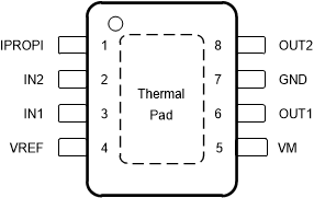
GUID-20201119-CA0I-NFQG-F5RT-FTZLD0MCGML6-low.gifFigure 6-1 DDA Package8-Pin HSOPTop View
Table 6-1 Pin Functions
PIN TYPE DESCRIPTION
NAME NO.
GND 7 PWR Device power ground. Connect to system ground.
IN1 3 I Logic inputs. Controls the H-bridge output. Has internal pulldowns. See Table 8-2.
IN2 2 I Logic inputs. Controls the H-bridge output. Has internal pulldowns. See Table 8-2.
IPROPI 1 PWR Analog current output proportional to load current. Section 8.4.2.1.
OUT1 6 O H-bridge output. Connect directly to the motor or other inductive load.
OUT2 8 O H-bridge output. Connect directly to the motor or other inductive load.
VM 5 PWR 4.5-V to 48-V power supply. Connect a 0.1-µF bypass capacitor to ground, as well as sufficient bulk capacitance, rated for the VM voltage.
VREF 4 I Analog input. Apply a voltage between 0 to 5 V. For information on current regulation, see the Section 8.4.2.1 section.
PAD Thermal pad. Connect to board ground. For good thermal dissipation, use large ground planes on multiple layers, and multiple nearby vias connecting those planes.