ZHCSI91B November   2017  – July 2018 DRV8304

UNLESS OTHERWISE NOTED, this document contains PRODUCTION DATA.  

  1. 特性
  2. 应用
  3. 说明
    1.     简化原理图
  4. 修订历史记录
  5. Pin Configuration and Functions
    1.     Pin Functions
  6. Specifications
    1. 6.1 Absolute Maximum Ratings
    2. 6.2 ESD Ratings
    3. 6.3 Recommended Operating Conditions
    4. 6.4 Thermal Information
    5. 6.5 Electrical Characteristics
    6. 6.6 Timing Requirements
    7. 6.7 Typical Characteristics
  7. Detailed Description
    1. 7.1 Overview
    2. 7.2 Functional Block Diagram
    3. 7.3 Feature Description
      1. 7.3.1 3-Phase Smart Gate Drivers
        1. 7.3.1.1 PWM Control Modes
          1. 7.3.1.1.1 6x PWM Mode (PWM_MODE = 00b or MODE Pin Tied to AGND)
          2. 7.3.1.1.2 3x PWM Mode (PWM_MODE = 01b or MODE Pin = 47 kΩ to AGND)
          3. 7.3.1.1.3 1x PWM Mode (PWM_MODE = 10b or MODE Pin = Hi-Z)
          4. 7.3.1.1.4 Independent PWM Mode (PWM_MODE = 11b or MODE Pin Tied to DVDD)
        2. 7.3.1.2 Device Interface Modes
          1. 7.3.1.2.1 Serial Peripheral Interface (SPI)
          2. 7.3.1.2.2 Hardware Interface
        3. 7.3.1.3 Gate Driver Voltage Supplies
        4. 7.3.1.4 Smart Gate-Drive Architecture
          1. 7.3.1.4.1 IDRIVE: MOSFET Slew-Rate Control
          2. 7.3.1.4.2 TDRIVE: MOSFET Gate Drive Control
          3. 7.3.1.4.3 Gate Drive Clamp
          4. 7.3.1.4.4 Propagation Delay
          5. 7.3.1.4.5 MOSFET VDS Monitors
          6. 7.3.1.4.6 VDRAIN Sense Pin
      2. 7.3.2 DVDD Linear Voltage Regulator
      3. 7.3.3 Pin Diagrams
      4. 7.3.4 Low-Side Current-Shunt Amplifiers
        1. 7.3.4.1 Bidirectional Current Sense Operation
        2. 7.3.4.2 Unidirectional Current Sense Operation (SPI only)
        3. 7.3.4.3 Offset Calibration
      5. 7.3.5 Gate-Driver Protection Circuits
        1. 7.3.5.1 VM Supply Undervoltage Lockout (UVLO)
        2. 7.3.5.2 VCP Charge-Pump Undervoltage Lockout (CPUV)
        3. 7.3.5.3 MOSFET VDS Overcurrent Protection (VDS_OCP)
          1. 7.3.5.3.1 VDS Latched Shutdown (OCP_MODE = 00b)
          2. 7.3.5.3.2 VDS Automatic Retry (OCP_MODE = 01b)
          3. 7.3.5.3.3 VDS Report Only (OCP_MODE = 10b)
          4. 7.3.5.3.4 VDS Disabled (OCP_MODE = 11b)
        4. 7.3.5.4 VSENSE Overcurrent Protection (SEN_OCP)
          1. 7.3.5.4.1 VSENSE Latched Shutdown (OCP_MODE = 00b)
          2. 7.3.5.4.2 VSENSE Automatic Retry (OCP_MODE = 01b)
          3. 7.3.5.4.3 VSENSE Report Only (OCP_MODE = 10b)
          4. 7.3.5.4.4 VSENSE Disabled (OCP_MODE = 11b or DIS_SEN = 1b)
        5. 7.3.5.5 Gate Driver Fault (GDF)
        6. 7.3.5.6 Thermal Warning (OTW)
        7. 7.3.5.7 Thermal Shutdown (OTSD)
    4. 7.4 Device Functional Modes
      1. 7.4.1 Gate Driver Functional Modes
        1. 7.4.1.1 Sleep Mode
        2. 7.4.1.2 Operating Mode
        3. 7.4.1.3 Fault Reset (CLR_FLT or ENABLE Reset Pulse)
    5. 7.5 Programming
      1. 7.5.1 SPI Communication
        1. 7.5.1.1 SPI
          1. 7.5.1.1.1 SPI Format
    6. 7.6 Register Maps
      1. Table 1. DRV8304S Register Map
      2. 7.6.1     Status Registers (DRV8304S Only)
        1. 7.6.1.1 Fault Status Register 1 (Address = 0x00) [reset = 0x00]
          1. Table 11. Fault Status Register 1 Field Descriptions
        2. 7.6.1.2 Fault Status Register 2 (Address = 0x01) [reset = 0x00]
          1. Table 12. Fault Status Register 2 Field Descriptions
      3. 7.6.2     Control Registers (DRV8304S Only)
        1. 7.6.2.1 Driver Control Register (Address = 0x02) [reset = 0x00]
          1. Table 14. Driver Control Field Descriptions
        2. 7.6.2.2 Gate Drive HS Register (Address = 0x03) [reset = 0x377]
          1. Table 15. Gate Drive HS Field Descriptions
        3. 7.6.2.3 Gate Drive LS Register (Address = 0x04) [reset = 0x777]
          1. Table 16. Gate Drive LS Register Field Descriptions
        4. 7.6.2.4 OCP Control Register (Address = 0x05) [reset = 0x145]
          1. Table 17. OCP Control Field Descriptions
        5. 7.6.2.5 CSA Control Register (Address = 0x06) [reset = 0x283]
          1. Table 18. CSA Control Field Descriptions
  8. Application and Implementation
    1. 8.1 Application Information
    2. 8.2 Typical Application
      1. 8.2.1 Primary Application
        1. 8.2.1.1 Design Requirements
        2. 8.2.1.2 Detailed Design Procedure
          1. 8.2.1.2.1 External MOSFET Support
            1. 8.2.1.2.1.1 Example
          2. 8.2.1.2.2 IDRIVE Configuration
            1. 8.2.1.2.2.1 Example
          3. 8.2.1.2.3 VDS Overcurrent Monitor Configuration
            1. 8.2.1.2.3.1 Example
          4. 8.2.1.2.4 Sense-Amplifier Bidirectional Configuration
            1. 8.2.1.2.4.1 Example
        3. 8.2.1.3 Application Curves
      2. 8.2.2 Alternative Application
        1. 8.2.2.1 Design Requirements
        2. 8.2.2.2 Detailed Design Procedure
          1. 8.2.2.2.1 Sense-Amplifier Unidirectional Configuration
            1. 8.2.2.2.1.1 Example
  9. Power Supply Recommendations
    1. 9.1 Bulk Capacitance Sizing
  10. 10Layout
    1. 10.1 Layout Guidelines
    2. 10.2 Layout Example
  11. 11器件和文档支持
    1. 11.1 器件支持
      1. 11.1.1 器件命名规则
    2. 11.2 文档支持
      1. 11.2.1 相关文档
    3. 11.3 接收文档更新通知
    4. 11.4 社区资源
    5. 11.5 商标
    6. 11.6 静电放电警告
    7. 11.7 术语表
  12. 12机械、封装和可订购信息

封装选项

请参考 PDF 数据表获取器件具体的封装图。

机械数据 (封装 | 引脚)
  • RHA|40
散热焊盘机械数据 (封装 | 引脚)
订购信息

TDRIVE: MOSFET Gate Drive Control

The TDRIVE component is an integrated gate-drive state machine that provides automatic dead-time insertion through switching handshaking, parasitic dV/dt gate turnon prevention, and MOSFET gate-fault detection.

The first component of the TDRIVE state machine is automatic dead-time insertion. Dead time is the period of time between the switching of the external high-side and low-side MOSFETs to ensure that they do not cross conduct and cause shoot-through. The DRV8304 device uses the VGS voltage monitors to measure the MOSFET gate-to-source voltage and determine the proper time to switch instead of relying on a fixed time value. This feature allows the gate-driver dead time to adjust for variation in the system such a temperature drift and variation in the MOSFET parameters. An additional digital dead time (tDEAD) can be inserted and is adjustable through the registers on the SPI device.

The second component focuses on parasitic dV/dt gate turnon prevention. To implement this, the TDRIVE state machine enables a strong pulldown current (ISTRONG) on the opposite MOSFET gate whenever a MOSFET is switching. The strong pulldown happens for the tDRIVE duration. This feature helps remove parasitic charge that couples into the MOSFET gate when the half-bridge switch-node voltage slews rapidly.

The third component implements a gate-fault detection scheme to detect pin-to-pin solder defects, a MOSFET gate failure, or a MOSFET gate stuck-high or stuck-low voltage condition. This implementation is done with a pair of VGS gate-to-source voltage monitors for each half-bridge gate driver. When the gate driver receives a command to change the state of the half-bridge it begins to monitor the gate voltage of the external MOSFET. If, at the end of the tDRIVE period, the VGS voltage has not reached the proper threshold, the gate driver reports a fault. To ensure that a false fault is not detected, a tDRIVE time should be selected that is longer than the time required to charge or discharge the MOSFET gate. The tDRIVE time does not increase the PWM time and will terminate if another PWM command is received while active. Additional details on the TDRIVE settings are described in the Register Maps section for SPI device and in the Pin Diagrams section for hardware interface device.

NOTE

If the mode is set to independent PWM mode, then the IDRIVE current is automatically set for the IHOLD period.

Figure 21 shows an example of the TDRIVE state machine in operation.
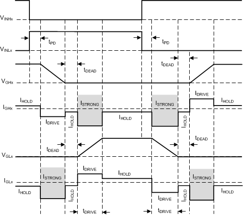
DRV8304 drv8304_t_drive_state_machine.gifFigure 21. TDRIVE State Machine