ZHCSI91B November 2017 – July 2018 DRV8304
UNLESS OTHERWISE NOTED, this document contains PRODUCTION DATA.
- 1 特性
- 2 应用
- 3 说明
- 4 修订历史记录
- 5 Pin Configuration and Functions
- 6 Specifications
-
7 Detailed Description
- 7.1 Overview
- 7.2 Functional Block Diagram
- 7.3
Feature Description
- 7.3.1 3-Phase Smart Gate Drivers
- 7.3.2 DVDD Linear Voltage Regulator
- 7.3.3 Pin Diagrams
- 7.3.4 Low-Side Current-Shunt Amplifiers
- 7.3.5 Gate-Driver Protection Circuits
- 7.4 Device Functional Modes
- 7.5 Programming
- 7.6
Register Maps
- Table 1. DRV8304S Register Map
- 7.6.1 Status Registers (DRV8304S Only)
- 7.6.2
Control Registers (DRV8304S Only)
- 7.6.2.1 Driver Control Register (Address = 0x02) [reset = 0x00]
- 7.6.2.2 Gate Drive HS Register (Address = 0x03) [reset = 0x377]
- 7.6.2.3 Gate Drive LS Register (Address = 0x04) [reset = 0x777]
- 7.6.2.4 OCP Control Register (Address = 0x05) [reset = 0x145]
- 7.6.2.5 CSA Control Register (Address = 0x06) [reset = 0x283]
- 8 Application and Implementation
- 9 Power Supply Recommendations
- 10Layout
- 11器件和文档支持
- 12机械、封装和可订购信息
封装选项
请参考 PDF 数据表获取器件具体的封装图。
机械数据 (封装 | 引脚)
- RHA|40
散热焊盘机械数据 (封装 | 引脚)
- RHA|40
订购信息
7.3.1.4.5 MOSFET VDS Monitors
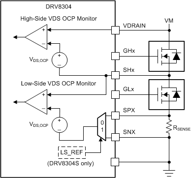
The gate drivers implement adjustable VDS voltage monitors to detect overcurrent or short-circuit conditions on the external power MOSFETs. When the monitored voltage is greater than the VDS trip point (VVDS_OCP) for longer than the deglitch time (tOCP), an overcurrent condition is detected and action is taken according to the device VDS fault mode.
The high-side VDS monitors measure the voltage between the VDRAIN and SHx pins and the low-side VDS monitors measure the voltage between the SHx and SPx pins. If the current shunt amplifier is unused, tie the SP pins to the common ground point of the external half-bridges.
For the SPI device, the reference point of the low-side VDS monitor can be changed between the SPx and SNx pins if desired with the LS_REF register setting.
The VVDS_OCP threshold is programmable from 0.15 V to 1.8 V. Additional information on the VDS monitor levels are described in the Register Maps section for the SPI device and in the Pin Diagrams section hardware interface device.
 Figure 23. DRV8304 VDS Monitors