ZHCSI91B November 2017 – July 2018 DRV8304
UNLESS OTHERWISE NOTED, this document contains PRODUCTION DATA.
- 1 特性
- 2 应用
- 3 说明
- 4 修订历史记录
- 5 Pin Configuration and Functions
- 6 Specifications
-
7 Detailed Description
- 7.1 Overview
- 7.2 Functional Block Diagram
- 7.3
Feature Description
- 7.3.1 3-Phase Smart Gate Drivers
- 7.3.2 DVDD Linear Voltage Regulator
- 7.3.3 Pin Diagrams
- 7.3.4 Low-Side Current-Shunt Amplifiers
- 7.3.5 Gate-Driver Protection Circuits
- 7.4 Device Functional Modes
- 7.5 Programming
- 7.6
Register Maps
- Table 1. DRV8304S Register Map
- 7.6.1 Status Registers (DRV8304S Only)
- 7.6.2
Control Registers (DRV8304S Only)
- 7.6.2.1 Driver Control Register (Address = 0x02) [reset = 0x00]
- 7.6.2.2 Gate Drive HS Register (Address = 0x03) [reset = 0x377]
- 7.6.2.3 Gate Drive LS Register (Address = 0x04) [reset = 0x777]
- 7.6.2.4 OCP Control Register (Address = 0x05) [reset = 0x145]
- 7.6.2.5 CSA Control Register (Address = 0x06) [reset = 0x283]
- 8 Application and Implementation
- 9 Power Supply Recommendations
- 10Layout
- 11器件和文档支持
- 12机械、封装和可订购信息
封装选项
请参考 PDF 数据表获取器件具体的封装图。
机械数据 (封装 | 引脚)
- RHA|40
散热焊盘机械数据 (封装 | 引脚)
- RHA|40
订购信息
7.3.4.1 Bidirectional Current Sense Operation
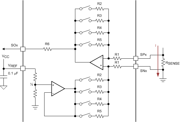
The SOx pin on the DRV8304 outputs an analog voltage equal to the voltage across the SPx and SNx pins multiplied by the gain setting (GCSA) as shown in Figure 30. The gain setting is adjustable between four different levels (5 V/V, 10 V/V, 20 V/V, and 40 V/V). Use Equation 3 to calculate the current through the shunt resistor.

 Figure 30. Bidirectional Current-Sense Configuration
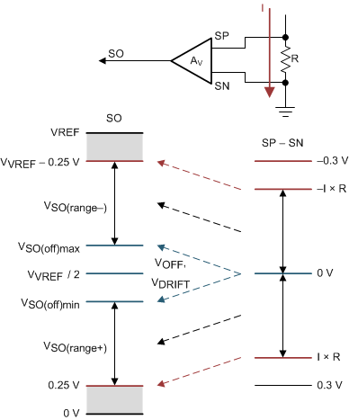
 Figure 31 and Figure 32 show the detail of the amplifier operational range. In bi-directional operation, the amplifier output for 0-V input is set at VREF / 2. Any change in the differential input results in a corresponding change in the output times the CSA_GAIN factor. The amplifier has a defined linear region in which it can maintain operation.
 Figure 31. Bidirectional Current-Sense Output
  Figure 32. Bidirectional Current Sense Regions