ZHCSF68D May   2015  – July 2019 DRV8305-Q1

PRODUCTION DATA.  

  1. 特性
  2. 应用
  3. 说明
    1.     Device Images
      1.      简化原理图
  4. 修订历史记录
  5. Pin Configuration and Functions
    1.     Pin Functions
  6. Specifications
    1. 6.1 Absolute Maximum Ratings
    2. 6.2 ESD Ratings
    3. 6.3 Recommended Operating Conditions
    4. 6.4 Thermal Information
    5. 6.5 Electrical Characteristics
    6. 6.6 SPI Timing Requirements (Slave Mode Only)
    7. 6.7 Typical Characteristics
  7. Detailed Description
    1. 7.1 Overview
    2. 7.2 Functional Block Diagram
    3. 7.3 Feature Description
      1. 7.3.1 Integrated Three-Phase Gate Driver
      2. 7.3.2 INHx/INLx: Gate Driver Input Modes
      3. 7.3.3 VCPH Charge Pump: High-Side Gate Supply
      4. 7.3.4 VCP_LSD LDO: Low-Side Gate Supply
      5. 7.3.5 GHx/GLx: Half-Bridge Gate Drivers
        1. 7.3.5.1 Smart Gate Drive Architecture: IDRIVE
        2. 7.3.5.2 Smart Gate Drive Architecture: TDRIVE
        3. 7.3.5.3 CSAs: Current Shunt Amplifiers
      6. 7.3.6 DVDD and AVDD: Internal Voltage Regulators
      7. 7.3.7 VREG: Voltage Regulator Output
      8. 7.3.8 Protection Features
        1. 7.3.8.1 Fault and Warning Classification
        2. 7.3.8.2 MOSFET Shoot-Through Protection (TDRIVE)
        3. 7.3.8.3 MOSFET Overcurrent Protection (VDS_OCP)
          1. 7.3.8.3.1 MOSFET dV/dt Turn On Protection (TDRIVE)
          2. 7.3.8.3.2 MOSFET Gate Drive Protection (GDF)
        4. 7.3.8.4 Low-Side Source Monitors (SNS_OCP)
        5. 7.3.8.5 Fault and Warning Operating Modes
      9. 7.3.9 Undervoltage Warning (UVFL), Undervoltage Lockout (UVLO), and Overvoltage (OV) Protection
        1. 7.3.9.1 Overtemperature Warning (OTW) and Shutdown (OTSD) Protection
        2. 7.3.9.2 Reverse Supply Protection
        3. 7.3.9.3 MCU Watchdog
        4. 7.3.9.4 VREG Undervoltage (VREG_UV)
        5. 7.3.9.5 Latched Fault Reset Methods
    4. 7.4 Device Functional Modes
      1. 7.4.1 Power Up Sequence
      2. 7.4.2 Standby State
      3. 7.4.3 Operating State
      4. 7.4.4 Sleep State
      5. 7.4.5 Limp Home or Fail Code Operation
    5. 7.5 Programming
      1. 7.5.1 SPI Communication
        1. 7.5.1.1 SPI
        2. 7.5.1.2 SPI Format
    6. 7.6 Register Maps
      1. 7.6.1 Status Registers
        1. 7.6.1.1 Warning and Watchdog Reset (Address = 0x1)
          1. Table 10. Warning and Watchdog Reset Register Description
        2. 7.6.1.2 OV/VDS Faults (Address = 0x2)
          1. Table 11. OV/VDS Faults Register Description
        3. 7.6.1.3 IC Faults (Address = 0x3)
          1. Table 12. IC Faults Register Description
        4. 7.6.1.4 VGS Faults (Address = 0x4)
          1. Table 13. Gate Driver VGS Faults Register Description
      2. 7.6.2 Control Registers
        1. 7.6.2.1 HS Gate Drive Control (Address = 0x5)
          1. Table 14. HS Gate Driver Control Register Description
        2. 7.6.2.2 LS Gate Drive Control (Address = 0x6)
          1. Table 15. LS Gate Driver Control Register Description
        3. 7.6.2.3 Gate Drive Control (Address = 0x7)
          1. Table 16. Gate Drive Control Register Description
        4. 7.6.2.4 IC Operation (Address = 0x9)
          1. Table 17. IC Operation Register Description
        5. 7.6.2.5 Shunt Amplifier Control (Address = 0xA)
          1. Table 18. Shunt Amplifier Control Register Description
        6. 7.6.2.6 Voltage Regulator Control (Address = 0xB)
          1. Table 19. Voltage Regulator Control Register Description
        7. 7.6.2.7 VDS Sense Control (Address = 0xC)
          1. Table 20. VDS Sense Control Register Description
  8. Application and Implementation
    1. 8.1 Application Information
    2. 8.2 Typical Application
      1. 8.2.1 Design Requirements
      2. 8.2.2 Detailed Design Procedure
        1. 8.2.2.1 Gate Drive Average Current
        2. 8.2.2.2 MOSFET Slew Rates
        3. 8.2.2.3 Overcurrent Protection
        4. 8.2.2.4 Current Sense Amplifiers
      3. 8.2.3 VREG Reference Voltage Input (DRV8305N)
      4. 8.2.4 Application Curves
  9. Power Supply Recommendations
    1. 9.1 Power Supply Consideration in Generator Mode
    2. 9.2 Bulk Capacitance
  10. 10Layout
    1. 10.1 Layout Guidelines
    2. 10.2 Layout Example
  11. 11器件和文档支持
    1. 11.1 文档支持
    2. 11.2 接收文档更新通知
    3. 11.3 社区资源
    4. 11.4 商标
    5. 11.5 静电放电警告
    6. 11.6 Glossary
  12. 12机械、封装和可订购信息

封装选项

机械数据 (封装 | 引脚)
散热焊盘机械数据 (封装 | 引脚)
订购信息

Power Supply Consideration in Generator Mode

When the motor shaft of BLDC or PMSM motor is turned by an external force, the motor windings will generate a voltage on the motor inputs. This condition is known as generator mode or motor back-drive. In the generator mode, a positive voltage can be observed on SHx pins of the device. If there is a switch between VDRAIN and PVDD (SWVDRAIN in Figure 24 ), and the following conditions exist in the system, the absolute maximum voltage of VCPH with respect to PVDD must be reviewed:

  • Generator mode
  • SWVDRAIN is off
  • PVDD and VCPH are low voltage (for example, PVDD = 0 V)

If SHx voltage (VSHx) exceeds the VCPH voltage, the VCPH voltage starts following VSHx because of the device internal diodes D1 and D2 (or D3). If the VCPH-PVDD voltage exceeds the absolute maximum voltage of DRV8305-Q1, the ESD diode D4 starts conducting, and results in a big current from SHx to PVDD through the diodes D2, D1, and D4. To avoid this condition, TI recommends to add an external diode DVDRAIN_PVDD between VDRAIN and PVDD.
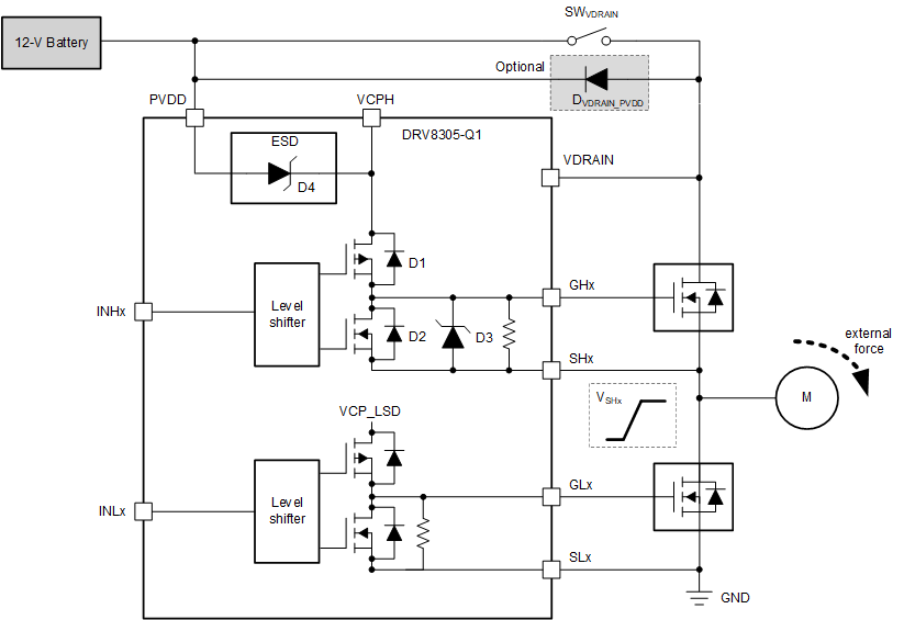
DRV8305-Q1 slvse12_generator_mode.gifFigure 24. Power Supply Consideration in Generator Mode