ZHCSE35 August 2015 DRV8305
PRODUCTION DATA.
- 1 特性
- 2 应用
- 3 说明
- 4 修订历史记录
- 5 Pin Configuration and Functions
- 6 Specifications
-
7 Detailed Description
- 7.1 Overview
- 7.2 Functional Block Diagram
- 7.3
Feature Description
- 7.3.1 Three-Phase Gate Driver
- 7.3.2 Operating Modes
- 7.3.3 Charge Pump
- 7.3.4 Gate Driver Architecture
- 7.3.5 IDRIVE/TDRIVE
- 7.3.6 Slew Rate/Slope Control
- 7.3.7 Current Shunt Amplifiers
- 7.3.8 Internal Regulators (DVDD and AVDD)
- 7.3.9 Voltage Regulator Output for Driving External Loads (VREG)
- 7.3.10 Protection Features
- 7.3.11
Undervoltage Reporting and Undervoltage Lockout (UVLO) Protection
- 7.3.11.1 Battery Overvoltage Protection (PVDD_OV)
- 7.3.11.2 Charge Pump Overvoltage Protection (VCPH_OV/VCP_LSD_OV)
- 7.3.11.3 Overtemperature (OT) Warning and Protection
- 7.3.11.4 dV/dt Protection
- 7.3.11.5 VGS Protection
- 7.3.11.6 Gate Driver Faults
- 7.3.11.7 Reverse Battery Protection
- 7.3.11.8 MCU Watchdog
- 7.3.12 Pin Control Functions
- 7.3.13 Fault / Warning Classes and Recovery
- 7.4 Device Functional Modes
- 7.5 Programming
- 7.6
Register Maps
- 7.6.1 Read / Write Bit
- 7.6.2 Status Registers
- 7.6.3 0x1 Warning and Watchdog Reset
- 7.6.4 0x2 OV/VDS Faults
- 7.6.5 0x3 IC Faults
- 7.6.6 0x4 Gate Driver VGS Faults
- 7.6.7
Control Registers
- 7.6.7.1 HS Gate Driver Control (address = 0x5)
- 7.6.7.2 LS Gate Driver Control (address = 0x6)
- 7.6.7.3 Gate Drive Control (address = 0x7)
- 7.6.7.4 IC Operation (address = 0x9)
- 7.6.7.5 Shunt Amplifier Control (address = 0xA)
- 7.6.7.6 Voltage Regulator Control (address = 0xB)
- 7.6.7.7 VDS Sense Control (address = 0xC)
- 8 Application and Implementation
- 9 Power Supply Recommendations
- 10Layout
- 11器件和文档支持
- 12机械、封装和可订购信息
9 Power Supply Recommendations
9.1 Bulk Capacitance
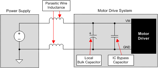
Having appropriate local bulk capacitance is an important factor in motor drive system design. It is generally beneficial to have more bulk capacitance, while the disadvantages are increased cost and physical size.
The amount of local capacitance needed depends on a variety of factors, including the:
- Highest current required by the motor system
- Power supply’s capacitance and ability to source or sink current
- Amount of parasitic inductance between the power supply and motor system
- Acceptable voltage ripple
- Type of motor used (brushed DC, brushless DC, stepper)
- Motor braking method
The inductance between the power supply and motor drive system will limit the rate current can change from the power supply. If the local bulk capacitance is too small, the system will respond to excessive current demands or dumps from the motor with a change in voltage. When adequate bulk capacitance is used, the motor voltage remains stable and high current can be quickly supplied.
The data sheet generally provides a recommended value, but system-level testing is required to determine the appropriate-sized bulk capacitor.
 Figure 16. Example Setup of Motor Drive System With External Power Supply
The voltage rating for bulk capacitors should be higher than the operating voltage, to provide margin for cases when the motor transfers energy to the supply.