ZHCSE35 August 2015 DRV8305
PRODUCTION DATA.
- 1 特性
- 2 应用
- 3 说明
- 4 修订历史记录
- 5 Pin Configuration and Functions
- 6 Specifications
-
7 Detailed Description
- 7.1 Overview
- 7.2 Functional Block Diagram
- 7.3
Feature Description
- 7.3.1 Three-Phase Gate Driver
- 7.3.2 Operating Modes
- 7.3.3 Charge Pump
- 7.3.4 Gate Driver Architecture
- 7.3.5 IDRIVE/TDRIVE
- 7.3.6 Slew Rate/Slope Control
- 7.3.7 Current Shunt Amplifiers
- 7.3.8 Internal Regulators (DVDD and AVDD)
- 7.3.9 Voltage Regulator Output for Driving External Loads (VREG)
- 7.3.10 Protection Features
- 7.3.11
Undervoltage Reporting and Undervoltage Lockout (UVLO) Protection
- 7.3.11.1 Battery Overvoltage Protection (PVDD_OV)
- 7.3.11.2 Charge Pump Overvoltage Protection (VCPH_OV/VCP_LSD_OV)
- 7.3.11.3 Overtemperature (OT) Warning and Protection
- 7.3.11.4 dV/dt Protection
- 7.3.11.5 VGS Protection
- 7.3.11.6 Gate Driver Faults
- 7.3.11.7 Reverse Battery Protection
- 7.3.11.8 MCU Watchdog
- 7.3.12 Pin Control Functions
- 7.3.13 Fault / Warning Classes and Recovery
- 7.4 Device Functional Modes
- 7.5 Programming
- 7.6
Register Maps
- 7.6.1 Read / Write Bit
- 7.6.2 Status Registers
- 7.6.3 0x1 Warning and Watchdog Reset
- 7.6.4 0x2 OV/VDS Faults
- 7.6.5 0x3 IC Faults
- 7.6.6 0x4 Gate Driver VGS Faults
- 7.6.7
Control Registers
- 7.6.7.1 HS Gate Driver Control (address = 0x5)
- 7.6.7.2 LS Gate Driver Control (address = 0x6)
- 7.6.7.3 Gate Drive Control (address = 0x7)
- 7.6.7.4 IC Operation (address = 0x9)
- 7.6.7.5 Shunt Amplifier Control (address = 0xA)
- 7.6.7.6 Voltage Regulator Control (address = 0xB)
- 7.6.7.7 VDS Sense Control (address = 0xC)
- 8 Application and Implementation
- 9 Power Supply Recommendations
- 10Layout
- 11器件和文档支持
- 12机械、封装和可订购信息
10 Layout
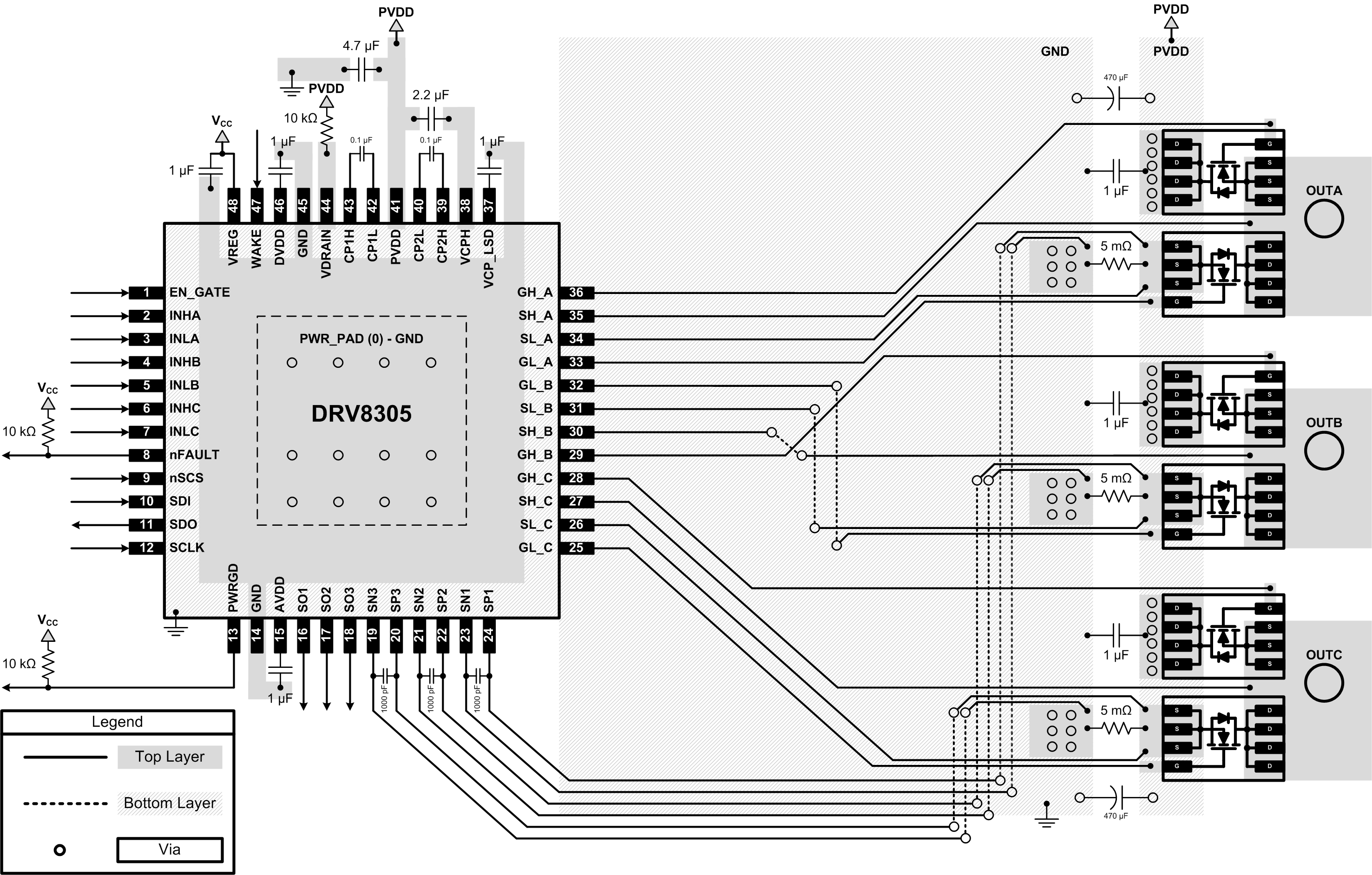
10.1 Layout Guidelines
Use the following layout recommendations when designing a PCB for the DRV8305.
- The DVDD and AVDD 1-μF bypass capacitors should connect directly to the adjacent GND pin to minimize loop impedance for the bypass capacitor.
- The CP1 and CP2 0.047-μF flying capacitors should be placed directly next to the DRV8305 charge pump pins.
- The VCPH 2.2-μF and VCP_LSD 1-μF bypass capacitors should be placed close to their corresponding pins with a direct path back to the DRV8305 GND net.
- The PVDD 4.7-μF bypass capacitor should be placed as close as possible to the DRV8305 PVDD supply pin.
- Use the proper footprint as shown in the 机械、封装和可订购信息 section.
- Minimize the loop length for the high-side and low-side gate drivers. The high-side loop is from the DRV8305 GH_X to the power MOSFET and returns through SH_X. The low-side loop is from the DRV8305 GL_X to the power MOSFET and returns through SL_X.
10.2 Layout Example
 Figure 17. Layout Recommendation