ZHCSE35 August 2015 DRV8305
PRODUCTION DATA.
- 1 特性
- 2 应用
- 3 说明
- 4 修订历史记录
- 5 Pin Configuration and Functions
- 6 Specifications
-
7 Detailed Description
- 7.1 Overview
- 7.2 Functional Block Diagram
- 7.3
Feature Description
- 7.3.1 Three-Phase Gate Driver
- 7.3.2 Operating Modes
- 7.3.3 Charge Pump
- 7.3.4 Gate Driver Architecture
- 7.3.5 IDRIVE/TDRIVE
- 7.3.6 Slew Rate/Slope Control
- 7.3.7 Current Shunt Amplifiers
- 7.3.8 Internal Regulators (DVDD and AVDD)
- 7.3.9 Voltage Regulator Output for Driving External Loads (VREG)
- 7.3.10 Protection Features
- 7.3.11
Undervoltage Reporting and Undervoltage Lockout (UVLO) Protection
- 7.3.11.1 Battery Overvoltage Protection (PVDD_OV)
- 7.3.11.2 Charge Pump Overvoltage Protection (VCPH_OV/VCP_LSD_OV)
- 7.3.11.3 Overtemperature (OT) Warning and Protection
- 7.3.11.4 dV/dt Protection
- 7.3.11.5 VGS Protection
- 7.3.11.6 Gate Driver Faults
- 7.3.11.7 Reverse Battery Protection
- 7.3.11.8 MCU Watchdog
- 7.3.12 Pin Control Functions
- 7.3.13 Fault / Warning Classes and Recovery
- 7.4 Device Functional Modes
- 7.5 Programming
- 7.6
Register Maps
- 7.6.1 Read / Write Bit
- 7.6.2 Status Registers
- 7.6.3 0x1 Warning and Watchdog Reset
- 7.6.4 0x2 OV/VDS Faults
- 7.6.5 0x3 IC Faults
- 7.6.6 0x4 Gate Driver VGS Faults
- 7.6.7
Control Registers
- 7.6.7.1 HS Gate Driver Control (address = 0x5)
- 7.6.7.2 LS Gate Driver Control (address = 0x6)
- 7.6.7.3 Gate Drive Control (address = 0x7)
- 7.6.7.4 IC Operation (address = 0x9)
- 7.6.7.5 Shunt Amplifier Control (address = 0xA)
- 7.6.7.6 Voltage Regulator Control (address = 0xB)
- 7.6.7.7 VDS Sense Control (address = 0xC)
- 8 Application and Implementation
- 9 Power Supply Recommendations
- 10Layout
- 11器件和文档支持
- 12机械、封装和可订购信息
6 Specifications
6.1 Absolute Maximum Ratings
over operating free-air temperature range referenced with respect to GND (unless otherwise noted) (1)| MIN | MAX | UNIT | |
|---|---|---|---|
| Power supply voltage (PVDD) | –0.3 | 45 | V |
| Power supply voltage ramp rate (VM) | 0 | 2 | V/µs |
| Charge pump voltage (CP1H,CP1L, CP2L,CP2H, VCPH, VCP_LSD) | –0.3 | PVDD + 12 | V |
| High side gate driver voltage (GHA, GHB, GHC) | –3 | 57 | V |
| Low-side gate driver voltage (GHA, GHB, GHC) | –2 | 12 | V |
| High side gate driver source pin voltage (SHA, SHB, SHC) | –5 | 45 | V |
| Low-side gate driver source pin voltage (SLA, SLB, SLC) | –3 | 5 | V |
| Internal phase clamp pin voltage difference {(GHA-SHA), (GHB-SHB), (GHC-SHC), (GLA-SLA), (GLB-SLB), (GLC-SLC)} | –0.3 | 15 | V |
| Drain pin voltage drain (VDRAIN) | –0.3 | 45 | V |
| Max source current (VDRAIN) – limit current with external series resistor | –20 | mA | |
| Max sink current (VDRAIN) | 2 | mA | |
| Voltage difference between supply and VDRAIN (PVDD-VDRAIN) | –10 | 10 | V |
| Control pin voltage range (INHA, INLA, INHB, INLB, INHC, INLC, EN_GATE, SCLK, SDI, SCS, SDO, nFAULT, PWRGD) | –0.3 | 5.5 | V |
| Open drain pins skink current (nFAULT, PWRGD) | 7 | mA | |
| Wake pin voltage (WAKE) | –0.3 | 45 | V |
| Wake pin sink current (WAKE) – limit with external series resistor | 1 | mA | |
| Sense amp voltage (SPA, SNA, SPB, SNB, SPC, SNC) | –2 | 5 | V |
| Externally applied reference voltage (VREG) – when vreg_vref = 1 | –0.3 | 5.5 | V |
| Externally applied reference sink current (VREG) – when vreg_vref = 1 | 100 | µA | |
| Operating ambient temperature, TA | –40 | 125 | °C |
| Operating junction temperature, TJ | –40 | 150 | °C |
| Storage temperature, Tstg | –55 | 150 | °C |
(1) Stresses beyond those listed under Absolute Maximum Ratings may cause permanent damage to the device. These are stress ratings only, which do not imply functional operation of the device at these or any other conditions beyond those indicated under Recommended Operating Conditions. Exposure to absolute-maximum-rated conditions for extended periods may affect device reliability.
6.2 ESD Ratings
| VALUE | UNIT | |||
|---|---|---|---|---|
| V(ESD) | Electrostatic discharge | Human-body model (HBM), per ANSI/ESDA/JEDEC JS-001 (1) | ±2000 | V |
| Charged-device model (CDM), per JEDEC specification JESD22-C101 (2) | ±500 | |||
(1) JEDEC document JEP155 states that 500-V HBM allows safe manufacturing with a standard ESD control process.
(2) JEDEC document JEP157 states that 250-V CDM allows safe manufacturing with a standard ESD control process.
6.3 Recommended Operating Conditions
over operating free-air temperature range (unless otherwise noted)| MIN | MAX | UNIT | ||
|---|---|---|---|---|
| VPVDD | Power supply voltage range | 4.4 | 45 (1) | V |
| VPVDD | Power supply voltage range for voltage regulator operation | 4.3 | 45 (2) | V |
| VPVDDRAMP | Power supply voltage ramp rate (PVDD = 0 to 20 V rising <3-mA pin sink current) | 1 | V/µs | |
| VPVDD-SH_X | Total voltage drop from PVDD to SH_X pins | 4.5 | V | |
| ISRC_VCPH | External load on VCPH pin (current limit resistor in series to load) | 10 | mA | |
| CO_OPA | Maximum external capacitive load on shunt amplifier (no external resistor on output, excluding internal pin capacitance) | 60 | pF | |
| InFAULT | nFAULT sink current (VnFAULT = 0.3 V) | 7 | mA | |
| Fgate | Operating switching frequency of gate driver | 200 | kHz | |
| IGATE | Total average gate driver current (HS + LS) – charge pump limited | 30 | mA | |
| TA | Operating ambient temperature | -40 | 125 | °C |
(1) IC is fully functional and tested in the range 4.4 to 45 V.
(2) Subject to thermal dissipation limits.
6.4 Thermal Information
| THERMAL METRIC (1) | DRV8305 | UNIT | |
|---|---|---|---|
| PHP (HTQFP) | |||
| 48 PINS | |||
| RθJA | Junction-to-ambient thermal resistance | 26.6 | °C/W |
| RθJC(top) | Junction-to-case (top) thermal resistance | 12.9 | °C/W |
| RθJB | Junction-to-board thermal resistance | 7.6 | °C/W |
| ψJT | Junction-to-top characterization parameter | 0.3 | °C/W |
| ψJB | Junction-to-board characterization parameter | 7.5 | °C/W |
| RθJC(bot) | Junction-to-case (bottom) thermal resistance | 0.6 | °C/W |
(1) For more information about traditional and new thermal metrics, see the Semiconductor and IC Package Thermal Metrics application report, SPRA953.
6.5 Electrical Characteristics
PVDD = 4.4 to 45 V, TJ = –40°C to 150°C, unless specified under test condition| PARAMETER | TEST CONDITIONS | MIN | TYP | MAX | UNIT | |
|---|---|---|---|---|---|---|
| POWER SUPPLIES (PVDD, DVDD, AVDD) | ||||||
| VPVDD | PVDD operating voltage | 4.4 | 45 | V | ||
| VREG (voltage regulator) operational | 4.3 | 45 | ||||
| IPVDD_Operating | PVDD operating supply current | EN_GATE = enabled; LDO reg = enabled at no load; outputs HiZ | 15 | mA | ||
| IPVDD_Standby | PVDD standby supply current | EN_GATE = disabled; LDO reg = enabled at no load | 4 | 7 | mA | |
| IPVDD_Sleep | PVDD sleep supply current | EN_GATE = disabled; LDO reg = disabled; ready for WAKE | 60 | 175 | μA | |
| VAVDD | Internal regulator voltage | PVDD = 5.3 to 45 V | 4.85 | 5 | 5.15 | V |
| PVDD = 4.4 to 5.3 V | PVDD – 0.22 | PVDD | ||||
| VDVDD | Internal regulator voltage | 3.3 | V | |||
| VOLTAGE REGULATOR (VREG) | ||||||
| VVREG | VREG DC output voltage | PVDD = 5.3 to 45 V | VSET – (0.03 × VSET) | VSET | VSET + (0.03 × VSET) | V |
| PVDD = 4.3 to 5.3 V; 5-V regulator | PVDD – 0.4 V | PVDD | ||||
| PVDD = 4.3 to 5.3 V; 3.3-V regulator | VSET – (0.03 × VSET) | VSET | VSET + (0.03 × VSET) | |||
| VLineReg | Line regulation ΔVOUT/ΔVIN | 5.3 V ≤ VIN ≤ 12 V; IO = 1 mA | 10 | 30 | mV | |
| VLoadReg | Load regulation ΔVOUT/ΔIOUT | 100 µA ≤ IOUT ≤ 50 mA | 30 | mV | ||
| Vdo | Dropout voltage | IOUT = 100 µA; 3.3 V | 0.05 | 0.1 | V | |
| IOUT = 50 mA; 3.3 V | 0.2 | 0.4 | ||||
| LOGIC-LEVEL INPUTS (INHA, INLA, INHB, INLB, INHC, INLC, EN_GATE, SCLK, nSCS) | ||||||
| VIL | Input logic low voltage | 0 | 0.8 | V | ||
| VIH | Input logic high voltage | 2 | 5 | V | ||
| RPD | Internal pull down resistor | To GND | 100 | kΩ | ||
| CONTROL OUTPUTS (nFAULT, SDO, PWRGD) | ||||||
| VOL | Output logic low voltage | IO = 5 mA | 0.5 | V | ||
| VOH | Output logic high voltage | 2.4 | V | |||
| IOH | Output logic high leakage | VO = 3.3 V | –1 | 1 | μA | |
| HIGH VOLTAGE TOLERANT LOGIC INPUT (WAKE) | ||||||
| VIL_WAKE | Output logic low voltage | 1.1 | 1.41 | V | ||
| VIH_WAKE | Output logic high voltage | 1.42 | 1.75 | V | ||
| GATE DRIVE OUTPUT (GHA, GHB, GHC, GLA, GLB, GLC) | ||||||
| VGHS | High side gate driver Vgs voltage | VPVDD = 8 to 45 V; IGATE < 30 mA, CVCPH = 2.2 μF, CCP1/CP2 = 0.047 μF, CVCP_LSD = 1 μF | 9 | 10 | 10.5 | V |
| VPVDD = 5.5 to 8 V; IGATE < 6 mA, CVCPH = 2.2 μF, CCP1/CP2 = 0.047 μF, CVCP_LSD = 1 μF | 7.2 | 9 | ||||
| VPVDD = 4.4 to 5.5 V; IGATE < 6 mA, CVCPH = 2.2 μF, CCP1/CP2 = 0.047 μF, CVCP_LSD = 1 μF | 5 | 7.2 | ||||
| VGLS | Low-side gate driver Vgs voltage | VPVDD = 8 to 45 V; IGATE < 30 mA, CVCPH = 2.2 μF, CCP1/CP2 = 0.047 μF, CVCP_LSD = 1 μF | 9 | 10 | 10.5 | V |
| VPVDD = 5.5 to 8 V; IGATE < 6 mA, CVCPH = 2.2 μF, CCP1/CP2 = 0.047 μF, CVCP_LSD = 1 μF | 9 | 10.5 | ||||
| VPVDD = 4.4 to 5.5 V; IGATE < 6 mA, CVCPH = 2.2 μF, CCP1/CP2 = 0.047 μF, CVCP_LSD = 1 μF | 8 | 9 | ||||
| PEAK CURRENT DRIVE TIMES | ||||||
| tDRIVE | Peak sink or source current drive time | TDRIVEP = 00; TDRIVEN = 00 | 220 | ns | ||
| TDRIVEP = 01; TDRIVEN = 01 | 440 | |||||
| TDRIVEP = 10; TDRIVEN = 10 | 880 | |||||
| TDRIVEP = 11; TDRIVEN = 11 | 1660 | |||||
| HIGH SIDE (GHA, GHB, GHC) PEAK CURRENT GATE DRIVE | ||||||
| IDRIVEP_HS | High side peak source current | IDRIVEP_HS = 0000 | 0.01 | A | ||
| IDRIVEP_HS = 0001 | 0.02 | |||||
| IDRIVEP_HS = 0010 | 0.03 | |||||
| IDRIVEP_HS = 0011 | 0.04 | |||||
| IDRIVEP_HS = 0100 | 0.05 | |||||
| IDRIVEP_HS = 0101 | 0.06 | |||||
| IDRIVEP_HS = 0110 | 0.07 | |||||
| IDRIVEP_HS = 0111 | 0.125 | |||||
| IDRIVEP_HS = 1000 | 0.25 | |||||
| IDRIVEP_HS = 1001 | 0.5 | |||||
| IDRIVEP_HS = 1010 | 0.75 | |||||
| IDRIVEP_HS = 1011 | 1 | |||||
| IDRIVEP_HS = 1100, 1101, 1110, 1111 | 0.05 | |||||
| IDRIVEN_HS | High side peak sink current | IDRIVEN_HS = 0000 | 0.02 | A | ||
| IDRIVEN_HS = 0001 | 0.03 | |||||
| IDRIVEN_HS = 0010 | 0.04 | |||||
| IDRIVEN_HS = 0011 | 0.05 | |||||
| IDRIVEN_HS = 0100 | 0.06 | |||||
| IDRIVEN_HS = 0101 | 0.07 | |||||
| IDRIVEN_HS = 0110 | 0.08 | |||||
| IDRIVEN_HS = 0111 | 0.25 | |||||
| IDRIVEN_HS = 1000 | 0.5 | |||||
| IDRIVEN_HS = 1001 | 0.75 | |||||
| IDRIVEN_HS = 1010 | 1 | |||||
| IDRIVEN_HS = 1011 | 1.25 | |||||
| IDRIVEN_HS = 1100, 1101, 1110, 1111 | 0.06 | |||||
| LOW SIDE (GLA, GLB, GLC) PEAK CURRENT GATE DRIVE | ||||||
| IDRIVEP_LS | Low-side peak source current | IDRIVEP_HS = 0000 | 0.01 | A | ||
| IDRIVEP_HS = 0001 | 0.02 | |||||
| IDRIVEP_HS = 0010 | 0.03 | |||||
| IDRIVEP_HS = 0011 | 0.04 | |||||
| IDRIVEP_HS = 0100 | 0.05 | |||||
| IDRIVEP_HS = 0101 | 0.06 | |||||
| IDRIVEP_HS = 0110 | 0.07 | |||||
| IDRIVEP_HS = 0111 | 0.125 | |||||
| IDRIVEP_HS = 1000 | 0.25 | |||||
| IDRIVEP_HS = 1001 | 0.5 | |||||
| IDRIVEP_HS = 1010 | 0.75 | |||||
| IDRIVEP_HS = 1011 | 1 | |||||
| IDRIVEP_HS = 1100, 1101, 1110, 1111 | 0.05 | |||||
| LOW SIDE (GLA, GLB, GLC) PEAK CURRENT GATE DRIVE | ||||||
| IDRIVEN_LS | Low-side peak sink current | IDRIVEN_HS = 0000 | 0.02 | A | ||
| IDRIVEN_HS = 0001 | 0.03 | |||||
| IDRIVEN_HS = 0010 | 0.04 | |||||
| IDRIVEN_HS = 0011 | 0.05 | |||||
| IDRIVEN_HS = 0100 | 0.06 | |||||
| IDRIVEN_HS = 0101 | 0.07 | |||||
| IDRIVEN_HS = 0110 | 0.08 | |||||
| IDRIVEN_HS = 0111 | 0.25 | |||||
| IDRIVEN_HS = 1000 | 0.5 | |||||
| IDRIVEN_HS = 1001 | 0.75 | |||||
| IDRIVEN_HS = 1010 | 1 | |||||
| IDRIVEN_HS = 1011 | 1.25 | |||||
| IDRIVEN_HS = 1100, 1101, 1110, 1111 | 0.06 | |||||
| GATE PULL DOWN, MOTOR OFF STATE (BRIDGE IN HI-Z) | ||||||
| RSLEEP_PD | Gate pull down resistance, SLEEP, under voltage and sleep mode | 2 V < PVDD < PVDD_UVLO2 GHX to GND; GLX to GND |
2000 | Ω | ||
| RSTANDBY_PD | Gate pull down resistance, STANDBY, standby mode (Parallel with ISTANDBY_PD) | PVDD > PVDD_UVLO2; EN_GATE = low; GHX to GND; GLX to GND |
750 | Ω | ||
| IOPERATING_PD | Gate pull down current, OPERATING, operating mode | PVDD > PVDD_UVLO2; EN_GATE = high; GHX to SHX; GLX to SLX |
50 | mA | ||
| GATE PULL DOWN, MOTOR ON STATE (IDRIVE/tdrive) | ||||||
| IHOLD | Gate pull down current, holding | PVDD > PVDD_UVLO2; EN_GATE = high; GHX to SHX; GLX to SLX |
50 | mA | ||
| IPULLDOWN | Gate pull down current, strong | PVDD > PVDD_UVLO2; EN_GATE = high; GHX to SHX; GLX to SLX |
1.25 | A | ||
| GATE TIMING | ||||||
| tpd_lf-O | Positive input falling to GHS_x falling | PVDD = 12 V; CL = 1 nF; 50% to 50% | 200 | ns | ||
| tpd_lr-O | Positive input rising to GHS_x rising | PVDD = 12 V; CL = 1 nF; 50% to 50% | 200 | ns | ||
| td_min | Minimum dead time after hand shaking | 280 | ns | |||
| tdtp | Dead time in addition to td_min | DEAD_TIME = 000 | 35 | ns | ||
| DEAD_TIME = 001 | 52 | |||||
| DEAD_TIME = 010 | 88 | |||||
| DEAD_TIME = 011 | 440 | |||||
| DEAD_TIME = 100 | 880 | |||||
| DEAD_TIME = 101 | 1760 | |||||
| DEAD_TIME = 110 | 3520 | |||||
| DEAD_TIME = 111 | 5280 | |||||
| tPD_MATCH | Propagation delay matching between high-side and low-side | 50 | ns | |||
| tDT_MATCH | Dead time matching | 50 | ns | |||
| CURRENT SHUNT AMPLIFIER | ||||||
| GCSA | Current sense amplifier gain | GAIN_CSx = 00 | 10 | V/V | ||
| GAIN_CSx = 01 | 20 | |||||
| GAIN_CSx = 10 | 40 | |||||
| GAIN_CSx = 11 | 80 | |||||
| GERR | Current sense amplifier gain error | Input differential > 0.025 V | –3% | 3% | ||
| tSETTLING | Current sense amplifier settling time | Settling time to 1%; no blanking; TJ = -40 – 150°C, GCSA = 10; Vstep = 0.46 V | 300 | ns | ||
| Settling time to 1%; no blanking; TJ = -40 – 150°C, GCSA = 20; Vstep = 0.46 V | 600 | |||||
| Settling time to 1%; no blanking; TJ = -40 – 150°C, GCSA = 40; Vstep = 0.46 V | 1.2 | µs | ||||
| Settling time to 1%; no blanking; TJ = -40 – 150°C, GCSA = 80; Vstep = 0.46 V | 2.4 | |||||
| VIOS | DC input offset | GCSA = 10; input shorted; RTI | –4 | 4 | mV | |
| VVREF_ERR | Reference buffer error (DC) | Internal or external VREF | –2% | 2% | ||
| VDRIFTOS | Input offset error drift | GCSA = 10; input shorted; RTI | 10 | µV/C | ||
| IBIAS | Input bias current | VIN_COM = 0; SOx open | 100 | µA | ||
| IOFFSET | Input bias current offset | IBIAS (SNx-SPx); VIN_COM = 0; SOx open | 1 | µA | ||
| VIN_COM | Common input mode range | –0.15 | 0.15 | V | ||
| VIN_DIFF | Differential input range | -0.48 | 0.48 | V | ||
| CMRR | Common mode rejection ration | External input resistance matched; DC; GCSA = 10 | 60 | 80 | dB | |
| External input resistance matched; 20 kHz; GCSA = 10 | 60 | 80 | ||||
| PSRR | Power supply rejection ratio | DC (<120 Hz); GCSA = 10 | 150 | dB | ||
| 20 kHz; GCSA = 10 | 90 | |||||
| VSWING | Output voltage swing | PVDD > 5.3 V | 0.3 | 4.7 | V | |
| VSLEW | Output slew rate | GCSA = 10; RL = 0 Ω; CL = 60 pF | 5.2 | 10 | V/µs | |
| IVO | Output short circuit current | SOx shorted to ground | 20 | mA | ||
| UGB | Unity gain bandwidth product | GCSA = 10 | 2 | MHz | ||
| VOLTAGE PROTECTION | ||||||
| VAVDD_UVLO | AVDD undervoltage Fault | Relative to GND | 3.3 | 3.5 | V | |
| VVREG_UV | VREG undervoltage Fault | VREG_UV_LEVEL = 00 | VSET-10% | V | ||
| VREG_UV_LEVEL = 01 | VSET-20% | |||||
| VREG_UV_LEVEL = 10 | VSET-30% | |||||
| VREG_UV_LEVEL = 11 | VSET-30% | |||||
| VVREG_UV_DGL | VREG undervoltage monitor deglitch time | 1.5 | 2 | µs | ||
| VPVDD_UVFL | Undervoltage protection Warning, PVDD | PVDD falling | 7.7 | 8.1 | V | |
| PVDD rising | 7.9 | 8.3 | ||||
| VPVDD_UVLO1 | Undervoltage protection lockout, PVDD | PVDD falling | 4.1 | V | ||
| PVDD rising | 4.3 | |||||
| VPVDD_UVLO2 | Undervoltage protection Fault, PVDD | PVDD falling | 4.2 | 4.4 | V | |
| PVDD rising | 4.4 | 4.6 | ||||
| VPVDD_OVFL | Overvoltage protection Warning, PVDD | PVDD falling | 33.5 | 36 | V | |
| PVDD rising | 32.5 | 35 | ||||
| VVCPH_UVFL | Charge pump under voltage protection Warning, VCPH | Relative to PVDD | 8 | V | ||
| VVCPH_UVLO | Charge pump under voltage protection Fault, VCPH | Relative to PVDD, SET_VCPH_UV = 0 | 4.5 | 4.9 | V | |
| Relative to PVDD, SET_VCPH_UV = 1 | 4.2 | 4.6 | ||||
| VVCP_LSD_UVLO | Low-side charge pump under voltage Fault, VCP_LSD | Relative to PVDD | 6.4 | 7.5 | V | |
| VVCPH_OVLO | Charge pump over voltage protection FAULT, VCPH | Relative to PVDD | 14 | 18 | V | |
| VVCPH_OVLO_ABS | Charge pump over voltage protection FAULT, VCPH | Relative to GND | 60 | V | ||
| TEMPERATURE PROTECTION | ||||||
| OTW_CLR | Junction temperature for resetting over temperature (OT) warning(1) | 140 | °C | |||
| OTW_SET/ OTSD_CLR |
Junction temperature for over temperature warning and resetting over temperature shutdown(1) | 155 | °C | |||
| OTSD_SET | Junction temperature for over temperature shutdown(1) | 175 | °C | |||
| TEMPFLAG1 | Junction temperature flag setting 1 (no warning)(1) | 105 | °C | |||
| TEMPFLAG2 | Junction temperature flag setting 2 (no warning)(1) | 125 | °C | |||
| TEMPFLAG3 | Junction temperature flag setting 3 (no warning)(1) | 135 | °C | |||
| TEMPFLAG4 | Junction temperature flag setting 4 (no warning)(1) | 175 | °C | |||
| PROTECTION CONTROL | ||||||
| tpd,E-L | Delay, error event to all gates low | 24 | µs | |||
| tpd,E-SD | Delay, error event to nFAULTx low | 7 | µs | |||
| FET CURRENT PROTECTION (VDS SENSING) | ||||||
| VDS_TRIP | Drain-source voltage protection limit | VDS_LEVEL = 00000 | 0.06 | V | ||
| VDS_LEVEL = 00001 | 0.068 | |||||
| VDS_LEVEL = 00010 | 0.076 | |||||
| VDS_LEVEL = 00011 | 0.086 | |||||
| VDS_LEVEL = 00100 | 0.097 | |||||
| VDS_LEVEL = 00101 | 0.109 | |||||
| VDS_LEVEL = 00110 | 0.123 | |||||
| VDS_LEVEL = 00111 | 0.138 | |||||
| VDS_LEVEL = 01000 | 0.155 | |||||
| VDS_LEVEL = 01001 | 0.175 | |||||
| VDS_LEVEL = 01010 | 0.197 | |||||
| VDS_LEVEL = 01011 | 0.222 | |||||
| VDS_LEVEL = 01100 | 0.25 | |||||
| VDS_LEVEL = 01101 | 0.282 | |||||
| VDS_LEVEL = 01110 | 0.317 | |||||
| VDS_LEVEL = 01111 | 0.358 | |||||
| VDS_LEVEL = 10000 | 0.403 | |||||
| VDS_LEVEL = 10001 | 0.454 | |||||
| VDS_LEVEL = 10010 | 0.511 | |||||
| VDS_LEVEL = 10011 | 0.576 | |||||
| VDS_LEVEL = 10100 | 0.648 | |||||
| VDS_LEVEL = 10101 | 0.73 | |||||
| VDS_LEVEL = 10110 | 0.822 | |||||
| VDS_LEVEL = 10111 | 0.926 | |||||
| VDS_LEVEL = 11000 | 1.043 | |||||
| VDS_LEVEL = 11001 | 1.175 | |||||
| VDS_LEVEL = 11010 | 1.324 | |||||
| VDS_LEVEL = 11011 | 1.491 | |||||
| VDS_LEVEL = 11100 | 1.679 | |||||
| VDS_LEVEL = 11101 | 1.892 | |||||
| VDS_LEVEL = 11110 | 2.131 | |||||
| VDS_LEVEL = 11111 | 2.131 | |||||
| tVDS | VDS sense deglitch time | TVDS = 00 | 0 | µs | ||
| TVDS = 01 | 1.75 | |||||
| TVDS = 10 | 3.5 | |||||
| TVDS = 11 | 7 | |||||
| tBLANK | VDS sense blanking time | TBLANK = 00 | 0 | µs | ||
| TBLANK = 01 | 1.75 | |||||
| TBLANK = 10 | 3.5 | |||||
| TBLANK = 11 | 7 | |||||
| tVDS_PULSE | nFAULT pin reporting pulse stretch length for VDS event | 56 | µs | |||
| PHASE SHORT PROTECTION | ||||||
| VSNSOCP_TRIP | Phase short protection limit | Fixed voltage | 2 | V | ||
(1) Specified by design and characterization data
6.6 SPI Timing Requirements (Slave Mode Only)
| MIN | NOM | MAX | UNIT | |||
|---|---|---|---|---|---|---|
| tSPI_READY | SPI read after power on | PVDD > VPVDD_UVLO1 | 5 | 10 | ms | |
| tCLK | Minimum SPI clock period | 100 | ns | |||
| tCLKH | Clock high time | 40 | ns | |||
| tCLKL | Clock low time | 40 | ns | |||
| tSU_SDI | SDI input data setup time | 20 | ns | |||
| tHD_SDI | SDI input data hold time | 30 | ns | |||
| tD_SDO | SDO output data delay time, CLK high to SDO valid | CL = 20 pF | 20 | ns | ||
| tHD_SDO | SDO output hold time | 40 | ns | |||
| tSU_SCS | SCS setup time | 50 | ns | |||
| tHD_SCS | SCS hold time | 50 | ns | |||
| tHI_SCS | SCS minimum high time before SCS active low | 400 | ns | |||
| tACC | SCS access time, SCS low to SDO out of high impedance | 10 | ns | |||
| tDIS | SCS disable time, SCS high to SDO high impedance | 10 | ns | |||
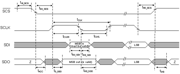 Figure 1. SPI Slave Mode Timing Definition
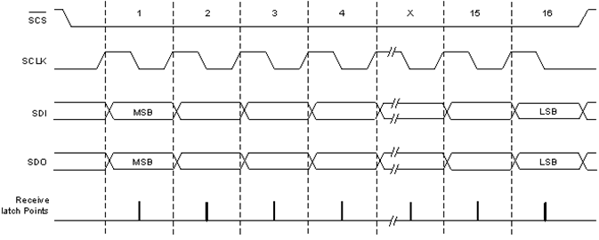 Figure 2. SPI Slave Mode Timing Diagram
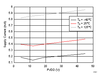
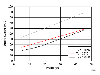
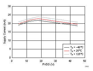
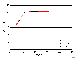
6.7 Typical Characteristics
