ZHCSHZ0A April 2018 – July 2018 DRV8306
PRODUCTION DATA.
- 1 特性
- 2 应用
- 3 说明
- 4 修订历史记录
- 5 Pin Configuration and Functions
- 6 Specifications
-
7 Detailed Description
- 7.1 Overview
- 7.2 Functional Block Diagram
- 7.3
Feature Description
- 7.3.1 Three Phase Smart Gate Drivers
- 7.3.2 DVDD Linear Voltage Regulator
- 7.3.3 Pulse-by-Pulse Current Limit
- 7.3.4 Hall Comparators
- 7.3.5 FGOUT Signal
- 7.3.6 Pin Diagrams
- 7.3.7 Gate-Driver Protective Circuits
- 7.4 Device Functional Modes
- 8 Application and Implementation
- 9 Power Supply Recommendations
- 10Layout
- 11器件和文档支持
- 12机械、封装和可订购信息
7.3.1.1 PWM Control Mode (1x PWM Mode)
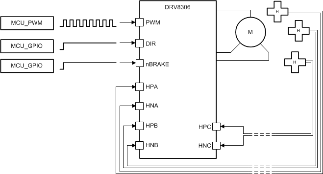
The DRV8306 device provides a 1x PWM control mode for driving the BLDC motor into trapezoidal current-control mode. The DRV8306 device uses 6-step block commutation tables that are stored internally. This feature lets a three-phase BLDC motor be controlled using a single PWM sourced from a simple controller. The PWM is applied on the PWM pin and determines the output frequency and duty cycle of the half-bridges.
The half-bridge output states are managed by the HPA, HNA, HPB, HNB, HPC and HNC pins which are used as state logic inputs. The state inputs are the position feedback of the BLDC motor. The device always operates with synchronous rectification.
The DIR pin controls the direction of BLDC motor in either clockwise or counter-clockwise direction. Tie the DIR pin low if this feature is not required.
The nBRAKE input halts the motor by turning off all high-side MOSFETs and turning on all low-side MOSFETs when it is pulled low. This brake is independent of the states of the other input pins. Tie the nBRAKE pin high if this feature is not required.
Table 2. Synchronous 1x PWM Mode
| HALL INPUTS | GATE-DRIVE OUTPUTS | ||||||||||||
|---|---|---|---|---|---|---|---|---|---|---|---|---|---|
| STATE | DIR = 0 | DIR = 1 | PHASE A | PHASE B | PHASE C | DESCRIPTION | |||||||
| HALL_A | HALL_B | HALL_C | HALL_A | HALL_B | HALL_C | GHA | GLA | GHB | GLB | GHC | GLC | ||
| Stop | 0 | 0 | 0 | 0 | 0 | 0 | L | L | L | L | L | L | Stop |
| Align | 1 | 1 | 1 | 1 | 1 | 1 | PWM | !PWM | L | H | L | H | Align |
| 1 | 1 | 1 | 0 | 0 | 0 | 1 | L | L | PWM | !PWM | L | H | B → C |
| 2 | 1 | 0 | 0 | 0 | 1 | 1 | PWM | !PWM | L | L | L | H | A → C |
| 3 | 1 | 0 | 1 | 0 | 1 | 0 | PWM | !PWM | L | H | L | L | A → B |
| 4 | 0 | 0 | 1 | 1 | 1 | 0 | L | L | L | H | PWM | !PWM | C → B |
| 5 | 0 | 1 | 1 | 1 | 0 | 0 | L | H | L | L | PWM | !PWM | C → A |
| 6 | 0 | 1 | 0 | 1 | 0 | 1 | L | H | PWM | !PWM | L | L | B → A |
Figure 9 shows the configuration in 1x PWM mode.
 Figure 9. 1x PWM Mode