ZHCSHZ0A April   2018  – July 2018 DRV8306

PRODUCTION DATA.  

  1. 特性
  2. 应用
  3. 说明
    1.     简化原理图
  4. 修订历史记录
  5. Pin Configuration and Functions
    1.     Pin Functions
  6. Specifications
    1. 6.1 Absolute Maximum Ratings
    2. 6.2 ESD Ratings
    3. 6.3 Recommended Operating Conditions
    4. 6.4 Thermal Information
    5. 6.5 Electrical Characteristics
    6. 6.6 Typical Characteristics
  7. Detailed Description
    1. 7.1 Overview
    2. 7.2 Functional Block Diagram
    3. 7.3 Feature Description
      1. 7.3.1 Three Phase Smart Gate Drivers
        1. 7.3.1.1 PWM Control Mode (1x PWM Mode)
        2. 7.3.1.2 Hardware Interface Mode
        3. 7.3.1.3 Gate Driver Voltage Supplies
        4. 7.3.1.4 Smart Gate Drive Architecture
          1. 7.3.1.4.1 IDRIVE: MOSFET Slew-Rate Control
          2. 7.3.1.4.2 TDRIVE: MOSFET Gate Drive Control
          3. 7.3.1.4.3 Gate Drive Clamp
          4. 7.3.1.4.4 Propagation Delay
          5. 7.3.1.4.5 MOSFET VDS Monitors
          6. 7.3.1.4.6 VDRAIN Sense Pin
      2. 7.3.2 DVDD Linear Voltage Regulator
      3. 7.3.3 Pulse-by-Pulse Current Limit
      4. 7.3.4 Hall Comparators
      5. 7.3.5 FGOUT Signal
      6. 7.3.6 Pin Diagrams
      7. 7.3.7 Gate-Driver Protective Circuits
        1. 7.3.7.1 VM Supply Undervoltage Lockout (UVLO)
        2. 7.3.7.2 VCP Charge-Pump Undervoltage Lockout (CPUV)
        3. 7.3.7.3 MOSFET VDS Overcurrent Protection (VDS_OCP)
        4. 7.3.7.4 VSENSE Overcurrent Protection (SEN_OCP)
        5. 7.3.7.5 Gate Driver Fault (GDF)
        6. 7.3.7.6 Thermal Shutdown (OTSD)
    4. 7.4 Device Functional Modes
      1. 7.4.1 Gate Driver Functional Modes
        1. 7.4.1.1 Sleep Mode
        2. 7.4.1.2 Operating Mode
        3. 7.4.1.3 Fault Reset (ENABLE Reset Pulse)
  8. Application and Implementation
    1. 8.1 Application Information
      1. 8.1.1 Hall Sensor Configuration and Connection
        1. 8.1.1.1 Typical Configuration
        2. 8.1.1.2 Open Drain Configuration
        3. 8.1.1.3 Series Configuration
        4. 8.1.1.4 Parallel Configuration
    2. 8.2 Typical Application
      1. 8.2.1 Primary Application
        1. 8.2.1.1 Design Requirements
        2. 8.2.1.2 Detailed Design Procedure
          1. 8.2.1.2.1 External MOSFET Support
            1. 8.2.1.2.1.1 Example
          2. 8.2.1.2.2 IDRIVE Configuration
            1. 8.2.1.2.2.1 Example
          3. 8.2.1.2.3 VDS Overcurrent Monitor Configuration
            1. 8.2.1.2.3.1 Example
        3. 8.2.1.3 Application Curves
  9. Power Supply Recommendations
    1. 9.1 Bulk Capacitance Sizing
  10. 10Layout
    1. 10.1 Layout Guidelines
    2. 10.2 Layout Example
  11. 11器件和文档支持
    1. 11.1 器件支持
      1. 11.1.1 器件命名规则
    2. 11.2 文档支持
      1. 11.2.1 相关文档
    3. 11.3 接收文档更新通知
    4. 11.4 社区资源
    5. 11.5 商标
    6. 11.6 静电放电警告
    7. 11.7 术语表
  12. 12机械、封装和可订购信息

封装选项

机械数据 (封装 | 引脚)
散热焊盘机械数据 (封装 | 引脚)
订购信息

Gate Driver Voltage Supplies

The high-side gate-drive voltage supply is created using a doubler charge pump that operates from the VM voltage supply input. The charge pump lets the gate driver correctly bias the high-side MOSFET gate with respect to its source across a wide input supply voltage range. The charge pump is regulated to maintain a fixed output voltage of VVM + 10 V and supports an average output current of 15 mA. When the VVM voltage is less than 12 V, the charge pump operates in full doubler mode and generates VVCP = 2 × VVM – 1.5 V when unloaded. The charge pump is continuously monitored for undervoltage to prevent under-driven MOSFET conditions. The charge pump requires a X5R or X7R, 1-µF, 16-V ceramic capacitor between the VM and VCP pins to act as the storage capacitor. Additionally, a X5R or X7R, 22-nF, VM-rated ceramic capacitor is required between the CPH and CPL pins to act as the flying capacitor.
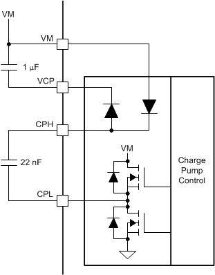
DRV8306 drv8306-charge-pump-architecture.gifFigure 11. Charge Pump Architecture

The low-side gate drive voltage is created using a linear low-dropout (LDO) regulator that operates from the VM voltage supply input. The LDO regulator allows the gate driver to properly bias the low-side MOSFET gate with respect to ground. The LDO regulator output is fixed at 10 V and supports an output current of 15 mA. The LDO regulator is monitored for undervoltage to prevent under-driven MOSFET conditions.