ZHCSHZ0A April   2018  – July 2018 DRV8306

PRODUCTION DATA.  

  1. 特性
  2. 应用
  3. 说明
    1.     简化原理图
  4. 修订历史记录
  5. Pin Configuration and Functions
    1.     Pin Functions
  6. Specifications
    1. 6.1 Absolute Maximum Ratings
    2. 6.2 ESD Ratings
    3. 6.3 Recommended Operating Conditions
    4. 6.4 Thermal Information
    5. 6.5 Electrical Characteristics
    6. 6.6 Typical Characteristics
  7. Detailed Description
    1. 7.1 Overview
    2. 7.2 Functional Block Diagram
    3. 7.3 Feature Description
      1. 7.3.1 Three Phase Smart Gate Drivers
        1. 7.3.1.1 PWM Control Mode (1x PWM Mode)
        2. 7.3.1.2 Hardware Interface Mode
        3. 7.3.1.3 Gate Driver Voltage Supplies
        4. 7.3.1.4 Smart Gate Drive Architecture
          1. 7.3.1.4.1 IDRIVE: MOSFET Slew-Rate Control
          2. 7.3.1.4.2 TDRIVE: MOSFET Gate Drive Control
          3. 7.3.1.4.3 Gate Drive Clamp
          4. 7.3.1.4.4 Propagation Delay
          5. 7.3.1.4.5 MOSFET VDS Monitors
          6. 7.3.1.4.6 VDRAIN Sense Pin
      2. 7.3.2 DVDD Linear Voltage Regulator
      3. 7.3.3 Pulse-by-Pulse Current Limit
      4. 7.3.4 Hall Comparators
      5. 7.3.5 FGOUT Signal
      6. 7.3.6 Pin Diagrams
      7. 7.3.7 Gate-Driver Protective Circuits
        1. 7.3.7.1 VM Supply Undervoltage Lockout (UVLO)
        2. 7.3.7.2 VCP Charge-Pump Undervoltage Lockout (CPUV)
        3. 7.3.7.3 MOSFET VDS Overcurrent Protection (VDS_OCP)
        4. 7.3.7.4 VSENSE Overcurrent Protection (SEN_OCP)
        5. 7.3.7.5 Gate Driver Fault (GDF)
        6. 7.3.7.6 Thermal Shutdown (OTSD)
    4. 7.4 Device Functional Modes
      1. 7.4.1 Gate Driver Functional Modes
        1. 7.4.1.1 Sleep Mode
        2. 7.4.1.2 Operating Mode
        3. 7.4.1.3 Fault Reset (ENABLE Reset Pulse)
  8. Application and Implementation
    1. 8.1 Application Information
      1. 8.1.1 Hall Sensor Configuration and Connection
        1. 8.1.1.1 Typical Configuration
        2. 8.1.1.2 Open Drain Configuration
        3. 8.1.1.3 Series Configuration
        4. 8.1.1.4 Parallel Configuration
    2. 8.2 Typical Application
      1. 8.2.1 Primary Application
        1. 8.2.1.1 Design Requirements
        2. 8.2.1.2 Detailed Design Procedure
          1. 8.2.1.2.1 External MOSFET Support
            1. 8.2.1.2.1.1 Example
          2. 8.2.1.2.2 IDRIVE Configuration
            1. 8.2.1.2.2.1 Example
          3. 8.2.1.2.3 VDS Overcurrent Monitor Configuration
            1. 8.2.1.2.3.1 Example
        3. 8.2.1.3 Application Curves
  9. Power Supply Recommendations
    1. 9.1 Bulk Capacitance Sizing
  10. 10Layout
    1. 10.1 Layout Guidelines
    2. 10.2 Layout Example
  11. 11器件和文档支持
    1. 11.1 器件支持
      1. 11.1.1 器件命名规则
    2. 11.2 文档支持
      1. 11.2.1 相关文档
    3. 11.3 接收文档更新通知
    4. 11.4 社区资源
    5. 11.5 商标
    6. 11.6 静电放电警告
    7. 11.7 术语表
  12. 12机械、封装和可订购信息

封装选项

机械数据 (封装 | 引脚)
散热焊盘机械数据 (封装 | 引脚)
订购信息

Typical Configuration

The Hall sensor inputs on the DRV8306 device can interface with a variety of Hall sensors. Typically, a Hall element is used, which outputs a differential signal on the order of 100 mV. To use this type of sensor, the DVDD regulator can be used to power the Hall sensor. Figure 26 shows the connections.
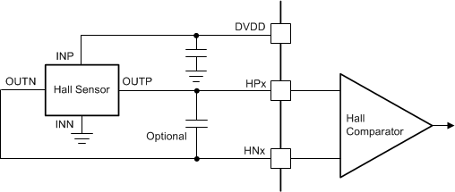
DRV8306 drv8306-typical-hall-sensor-configuration.gifFigure 26. Typical Hall Sensor Configuration

Because the amplitude of the Hall-sensor output signal is very low, capacitors are often placed across the Hall inputs to help reject noise coupled from the motor. Capacitors with a value of 1 nF to 100 nF are typically used.