ZHCSC39B February 2014 – November 2017 DRV8308
PRODUCTION DATA.
- 1 特性
- 2 应用
- 3 说明
- 4 修订历史记录
- 5 Pin Configurations and Functions
- 6 Specifications
-
7 Detailed Description
- 7.1 Overview
- 7.2 Functional Block Diagram
- 7.3
Feature Description
- 7.3.1 Hall Comparators
- 7.3.2 FG Amplifier, Comparator, and FG Output
- 7.3.3 Enable, Reset, and Clock Generation
- 7.3.4 Commutation
- 7.3.5 Commutation Logic Block Diagram
- 7.3.6 Commutation Parameters
- 7.3.7 Braking
- 7.3.8 Output Pre-Drivers
- 7.3.9 Current Limit
- 7.3.10 Charge Pump
- 7.3.11 5-V Linear Regulator
- 7.3.12 Power Switch
- 7.3.13 Protection Circuits
- 7.4 Device Functional Modes
- 7.5 Programming
- 7.6 Register Map
- 8 Application and Implementation
- 9 Power Supply Recommendations
- 10Layout
- 11器件和文档支持
- 12机械、封装和可订购信息
8 Application and Implementation
NOTE
Information in the following applications sections is not part of the TI component specification, and TI does not warrant its accuracy or completeness. TI’s customers are responsible for determining suitability of components for their purposes. Customers should validate and test their design implementation to confirm system functionality.
8.1 Application Information
8.1.1 Internal Speed Control Loop Constraints
The DRV8308 device is a versatile speed controller and driver for small, 3-phase brushless motors. However, there are some limitations to its application.
The built-in speed control loop is designed to work optimally with motor electrical speeds from about 50 Hz up to 6.7 kHz. For an 8-pole motor, this translates into about 500 RPM up to more than 100000 RPM. For motors with higher pole counts, these speeds scale down; for lower pole counts, they scale up.
Operation is possible at slower or faster speeds, but speed control becomes less effective, especially if using the Hall sensors for speed feedback (as opposed to the FG input).
Typically, the speed loop is optimized (by setting the filter coefficients and gains) at one desired motor speed. Operation is possible with one set of parameters over a limited speed range (for example, 1000 RPM to 2000 RPM), However, operation over a very wide speed range requires different parameters. The use of the auto gain and auto advance features can extend the dynamic range up to 4×.
When using the SPI interface to program the registers, the parameters can be updated at any time, even while the motor is running. In this manner, a wider range of speeds can be accommodated by the speed loop.
When not using the internal speed loop (when controlling the motor using PWM input or register speed control), the limits imposed by the speed loop do not apply. An external speed control implementation (using a microcontroller, FPGA, or other logic) can essentially control the motor current directly.
However, if using sine commutation, there are limits to the minimum and maximum speed, which are dictated by the timers that are used to generate the commutation sequence. The commutation timer is a 25-bit timer clocked at 50 MHz; therefore, the longest time it can capture is 655 ms. This limits the slowest speed to about 1.5 Hz (or 23 RPM for an 8-pole motor). At the other extreme, there are 960 steps in each sine commutation cycle. To ensure that there is enough time for the steps, the maximum speed is that which generates 960 counts at 50 MHz, or 52 kHz. This corresponds to a maximum speed of 800000 RPM for an 8-pole motor.
When not using the internal speed loop and using 120° commutation (using all three Hall sensors), there are no speed limitations. Commutation is performed with combinational logic.
8.1.2 Hall Sensor Configurations and Connections
The Hall sensor inputs on the DRV8308 device are capable of interfacing with a variety of Hall sensors. Typically, a Hall element is used, which outputs a differential signal on the order of 100 mV. To use this type of sensor, the VREG5 regulator can be used to power the Hall sensor. Connections are as shown in Figure 25:
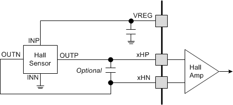 Figure 25. Hall Sensor Connections
Since the amplitude of the Hall sensor output signal is very low, often capacitors are placed across the Hall inputs to help reject noise coupled from the motor PWM. Typically capacitors from 1 to 100 nF are used.
Some motors use digital Hall sensors with open-drain outputs. These sensors can also be used with the DRV8308 device, with the addition of a few resistors:
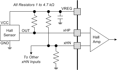 Figure 26. Hall Resistors
The negative (xHN) inputs are biased to 2.5 V by a pair of resistors between VREG and ground. For open-collector Hall sensors, an additional pullup resistor to VREG is needed on the positive (xHP) input. Again, the VREG output can usually be used to supply power to the Hall sensors.
8.1.3 FG Amplifier Configurations and Connections
To improve speed control by providing a higher bandwidth speed feedback, often a magnetic pickup coil, commonly referred to as an FG generator, is used. This is typically implemented as a serpentine PCB trace on the motor PCB. This generates a low-level sine wave signal whose amplitude and frequency is proportional to the speed of the motor.
Since the FG trace is in close proximity to the motor coils, it is very susceptible to noise coupling from the PWM of the motor. Noise coupling into the FG circuit causes poor speed regulation, especially at low motor speeds. Startup is a particularly difficult situation, as the motor current is at a maximum, and the FG signal amplitude is low (in fact, 0 at the moment of startup). If noise couples into FG during startup, the speed loop interprets the noise as fast motor rotation, and lowers the PWM duty cycle. The result is slow startup of the motor. If this problem is suspected, looking at the FGOUT signal with an oscilloscope during startup should reveal it.
To address this, in addition to the resistors that set the gain of the FG amplifier (R1 and R2 in Figure 27), usually passive filter components are needed on the FG amplifier circuit.
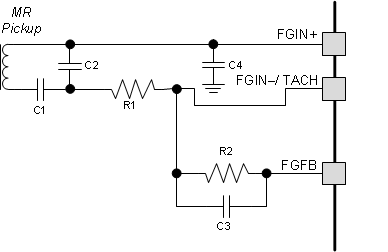 Figure 27. FG Amplifier Circuit
Ideally, the user desires a large amount of rejection of the PWM frequency. However, the user needs to pass the frequency that corresponds to their fastest motor speed. As an example, a motor may put out 36 FG pulses per revolution. At 5000 RPM, this is a 3-kHz signal. If you operate the PWM at 25 kHz, you can set a single pole at 3 kHz and have significant rejection of the PWM frequency, and the higher harmonics of the PWM (which are typically more easily coupled) are rejected even more.
Because the amplitude of the FG signal also increases with higher motor speed, it is possible to set this pole at a much lower frequency than the maximum speed dictates. The optimal values need to be determined by testing on the actual motor.
This pole is set by C3 in Figure 27.
In addition to rejection of high frequency, the FG winding should be AC-coupled to the amplifier to prevent any issues with DC offsets. This capacitor (C1) must be large enough to allow the motor to start-up reliably, since the FG frequency and amplitude are very low at startup. Typically capacitors on the order of 100 nF to 1 µF are used here. The voltage is low, so a 6.3-V ceramic capacitor can be used.
Occasionally an additional small capacitor is used across the FG trace. This capacitor (C2 above) may not be needed, but it can help reject very high-frequency harmonics of the PWM (glitches). Capacitors between 330 and 2200 pF are typically used.
8.2 Typical Application
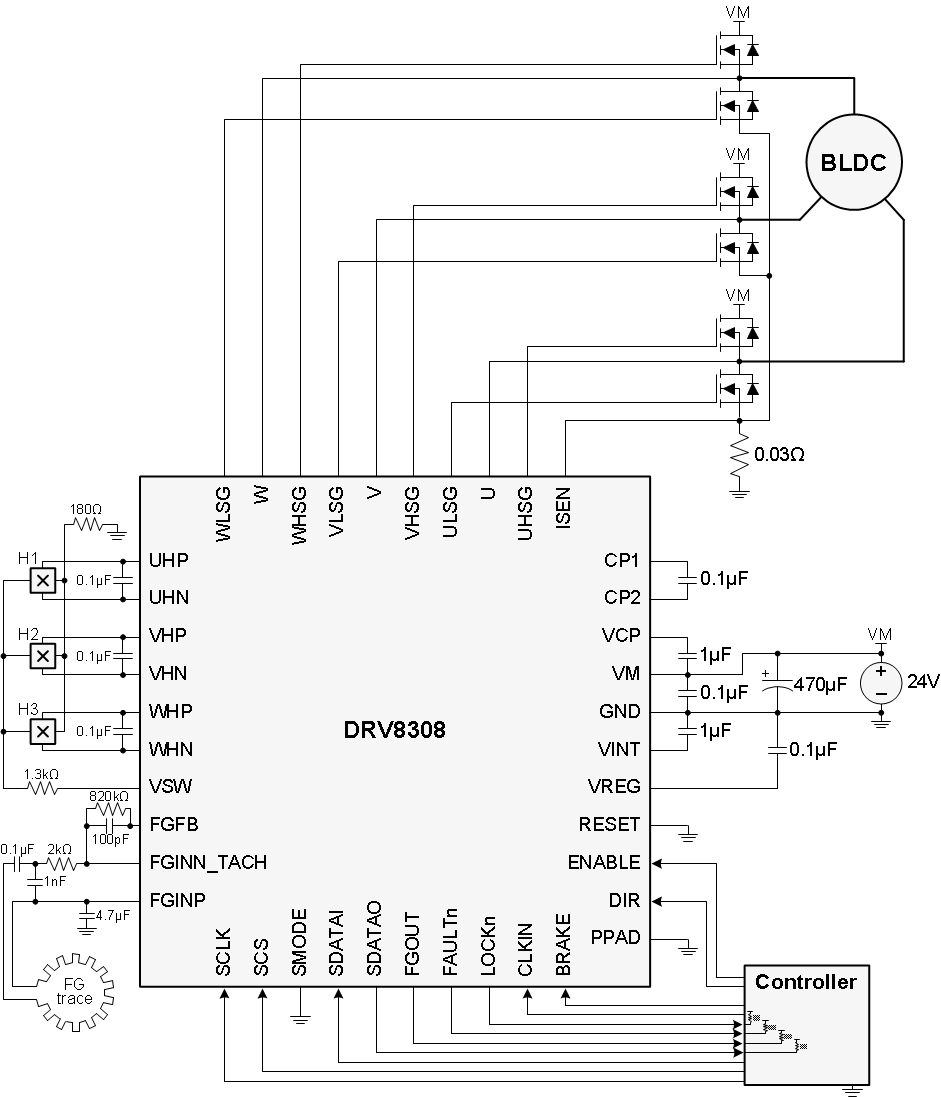 Figure 28. Typical Application
8.2.1 Design Requirements
This section describes design considerations.
| DESIGN PARAMETER | REFERENCE | EXAMPLE VALUE |
|---|---|---|
| Motor voltage | VM | 24V |
| Motor current (peak and RMS) | IM | 10A peak, 3A RMS |
| Speed command method | speed | Closed-loop at 3000 RPM |
| Required flutter (speed jitter) | flutter | < 0.2% |
| Configuration method | config | Use OTP |
| Hall element current | IHALL | 7mA |
| Power FET switching time | tFET | 500ns |
8.2.2 Detailed Design Procedure
8.2.2.1 Motor voltage
BLDC motors are typically rated for a certain voltage. Higher voltages generally have the advantage of causing current to change faster through the inductive windings, which allows for higher RPMs. And for a given required power delivery (torque * speed), higher voltage allows for lower current.
8.2.2.2 Motor Current (Peak and RMS)
It is important to understand and control motor current. This affects power FET device selection, the amount of required bulk capacitance, and the sizing of the sense resistor for the DRV8308 current-limiter feature.
With BLDC motors, increasing the load torque increases current. For a fixed load, the current during motor spin-up is the highest. It is generally a good idea to limit spin-up current by sizing sense resistors appropriately, because if it’s not limited, a motor can consume many amperes during startup and cause VM to droop unless a large amount of bulk capacitance is used. Limiting current reduces the bulk capacitance required.
The DRV8308 VLIMITER trips at 0.25V. If the sense resistance is 0.025Ω for example, 10A will be required to raise the ISEN voltage above 0.25V. When this happens, the DRV8308 drives the external FETs with a shorter duty cycle to limit current below 10A.
When selecting the power FET device, key parameters to consider are:
- It must be N-channel type, and 6 are needed.
- The max drain current (ID); pulsed and continuous.
- Max VDS must be greater than VM.
- Max VGS must be at least 12V (the DRV8308 drives approximately 10V).
- RDS(ON) – lower values decrease device temperature.
8.2.2.3 Speed Command Method
The DRV8308 can drive BLDCs using an open-loop 0% to 100% command, or using closed-loop speed control. When using closed-loop, the correct reference clock frequency (on CLKIN) must be calculated.
If DRV8308 register FGSEL is set to 00b to use Hall U to sense motor speed,

NPOLES is the number of permanent magnet poles.
If DRV8308 register FGSEL is set to 10b to use FG to sense motor speed,

NFG is the number of FG cycles per motor revolution.
8.2.2.4 Required Flutter (Speed Jitter)
Flutter is a measure of motor speed consistency. The best possible flutter largely depends on motor characteristics, loading, and tuning of the DRV8308 registers. BLDC motors with high detent torque and discrete positions will have higher flutter. The DRV8308EVM User's Guide SLVUA41 describes the important registers and a tuning process.
8.2.2.5 Configuration Method
The DRV8308 must have its registers set in order to function. There are 3 methods:
- Pre-program an external EEPROM, and set pin SMODE High.
- Set pin SMODE Low, and write register data over SPI while the DRV8308 is powered.
- Set pin SMODE Low, write register data over SPI while the DRV8308 is powered, and burn it to the internal EPROM (OTP). Then on future power ups, the DRV8308 will load the custom configuration data.
If the DRV8308 will be used in an open-loop PWM mode, the following register settings provide good baseline settings:
| ADDRESS | VALUE |
|---|---|
| 0x00 | 0x0911 |
| 0x01 | 0x0000 |
| 0x02 | 0x04FF |
| 0x03 | 0x6800 |
| 0x04 | 0x40D2 |
| 0x05 | 0x0000 |
| 0x06 | 0x0000 |
| 0x07 | 0x0000 |
| 0x08 | 0x0000 |
| 0x09 | 0x0000 |
| 0x0A | 0xF000 |
| 0x0B | 0x0000 |
8.2.2.6 Hall Element Current
Hall elements output a differential voltage that is proportional to the amount of bias current. An absolute max current is specified, as well as the element resistance over temperature.
The DRV8308 regulated outputs VREG or VSW can be used to supply Hall element current, along with a series resistor to limit element current. Its sizing depends on the element equivalent resistance (they can be arranged in parallel or serial), and the VM voltage if VSW is used.
8.2.2.7 Power FET Switching Time
The switching time on the external FETs is the VGS rise time, and it can be easily controlled with DRV8308 register IDRIVE. The 10mA setting causes a switching time that is 5 times the 50mA setting. Larger FETs that have higher current capabilities have a larger gate charge (Qg), and require higher IDRIVE settings for reasonable switching times.
However, fast switching times can cause extra voltage noise on VM and GND. This can be especially due to a relatively slow reverse-recovery time of the low-side body diode, where it conducts reverse-bias momentarily, being similar to shoot-through. To minimize noise, lower IDRIVE settings are often beneficial, and the 10mA setting has worked well with many types of FETs operating below 5A.
8.2.3 Application Curves
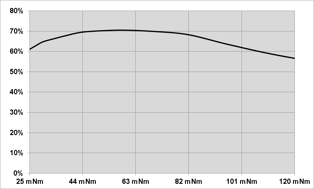 Figure 29. Closed-loop Efficiency vs Torque
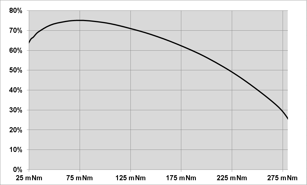 Figure 31. Open-loop Efficiency vs Torque
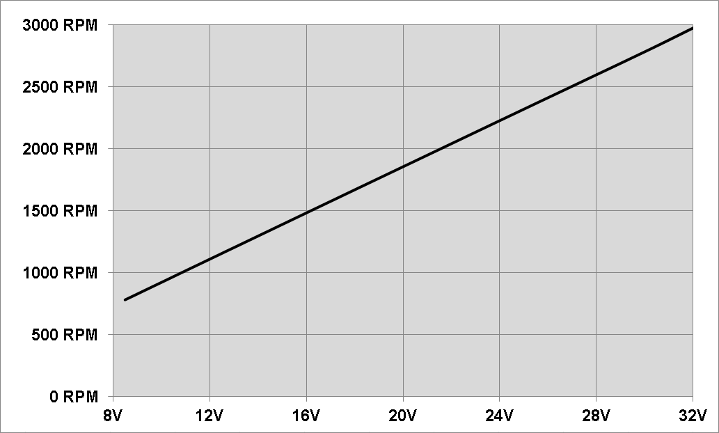
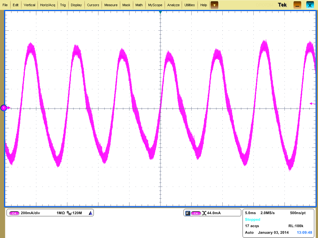
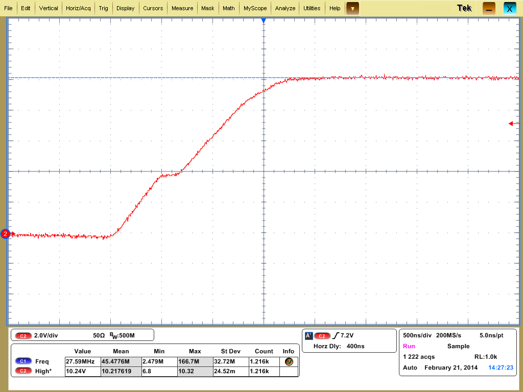 Figure 37. Vgs with IDRIVE = 10mA
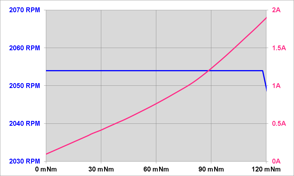 Figure 30. Closed-loop RPM and Current vs Torque
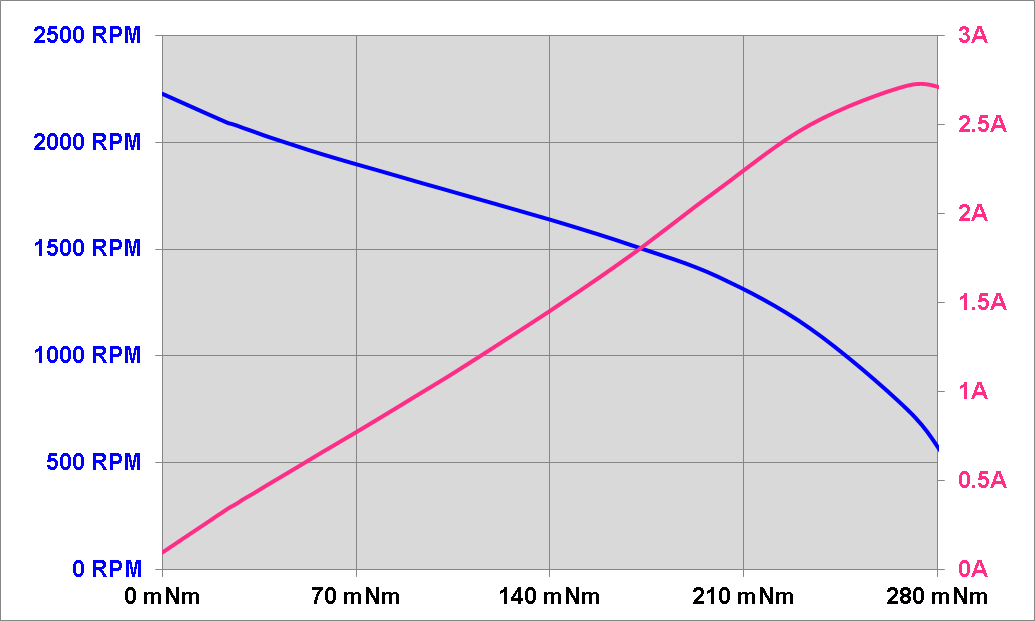 Figure 32. Open-loop RPM and Current vs Torque
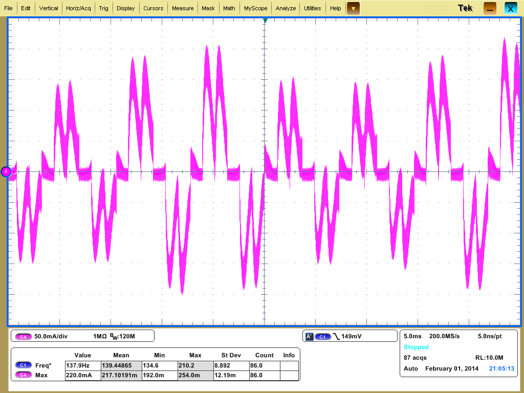
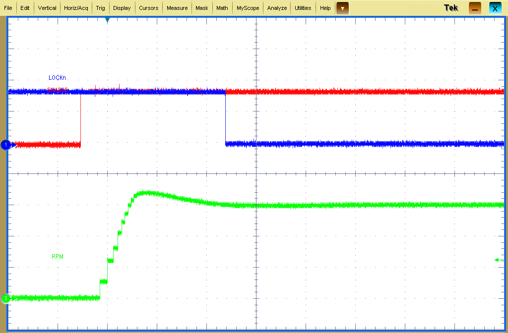
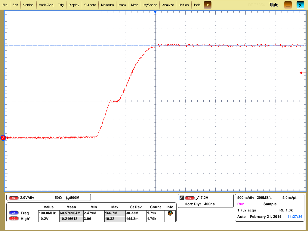 Figure 38. Vgs with IDRIVE = 20mA
8.3 Do's and Don'ts
8.3.1 RESET and ENABLE Considerations
Since the ENABLE function doubles as a sleep (low-power shutdown) function, there are some important considerations when asserting and deasserting ENABLE and RESET.
While the motor driver is enabled, the deassertion of ENABLE initiates a stop-and-power-down sequence. This sequence starts by disabling the motor (either braking or coasting depending on the BRKMOD bit), and waiting for rotation to stop. After rotation is stopped for 1 s (as determined by the absence of transitions on FGOUT), the internal circuitry is powered-down, the V5 regulator and power switch are disabled, and internal clocks are stopped.
In this low-power sleep state, the serial interface may still be used to read or write registers. All other logic is disabled.
After this stop-and-power-down sequence has been initiated (by deasserting the ENABLE pin for at least 1.2 µs, or by changing the state of the ENPOL bit), the sequence continues to completion, regardless of the state of ENABLE. If ENABLE is immediately returned to the active state, the motor slows and stops for 1 s, at which point it starts again.
If RESET is asserted during power-down (at any time after the deassertion of ENABLE is recognized), it is acted upon when ENABLE is again asserted, and the part powers-up.
If RESET is asserted when ENABLE is active, the motor is stopped similar to the sequence when ENABLE is deasserted. After it is stopped for 1 s, all internal registers are reloaded with the value contained in OTP memory, faults are cleared, and internal states (that is, the speed loop datapath) are initialized. The motor remains disabled until RESET is deasserted.
RESET and ENABLE may be connected together (if the ENPOL bit in OTP memory is programmed so that ENABLE is active low). When both signals are low, the motor is enabled; when both signals are high, the motor is disabled. As soon as the signals are returned to high, all registers are reloaded from OTP memory, faults are cleared, and the motor starts.