ZHCSOY8B September   2021  – February 2022 DRV8311

PRODUCTION DATA  

  1. 特性
  2. 应用
  3. 说明
  4. Revision History
  5. Device Comparison Table
  6. Pin Configuration and Functions
  7. Specifications
    1. 7.1 Absolute Maximum Ratings
    2. 7.2 ESD Ratings
    3. 7.3 Recommended Operating Conditions
    4. 7.4 Thermal Information
    5. 7.5 Electrical Characteristics
    6. 7.6 SPI Timing Requirements
    7. 7.7 SPI Secondary Device Mode Timings
    8. 7.8 Typical Characteristics
  8. Detailed Description
    1. 8.1 Overview
    2. 8.2 Functional Block Diagram
    3. 8.3 Feature Description
      1. 8.3.1  Output Stage
      2. 8.3.2  Control Modes
        1. 8.3.2.1 6x PWM Mode (DRV8311S and DRV8311H variants only)
        2. 8.3.2.2 3x PWM Mode (DRV8311S and DRV8311H variants only)
        3. 8.3.2.3 PWM Generation Mode (DRV8311S and DRV8311P Variants)
      3. 8.3.3  Device Interface Modes
        1. 8.3.3.1 Serial Peripheral Interface (SPI)
        2. 8.3.3.2 Hardware Interface
      4. 8.3.4  AVDD Linear Voltage Regulator
      5. 8.3.5  Charge Pump
      6. 8.3.6  Slew Rate Control
      7. 8.3.7  Cross Conduction (Dead Time)
      8. 8.3.8  Propagation Delay
      9. 8.3.9  Pin Diagrams
        1. 8.3.9.1 Logic Level Input Pin (Internal Pulldown)
        2. 8.3.9.2 Logic Level Input Pin (Internal Pullup)
        3. 8.3.9.3 Open Drain Pin
        4. 8.3.9.4 Push Pull Pin
        5. 8.3.9.5 Four Level Input Pin
      10. 8.3.10 Current Sense Amplifiers
        1. 8.3.10.1 Current Sense Amplifier Operation
        2. 8.3.10.2 Current Sense Amplifier Offset Correction
      11. 8.3.11 Protections
        1. 8.3.11.1 VM Supply Undervoltage Lockout (NPOR)
        2. 8.3.11.2 Under Voltage Protections (UVP)
        3. 8.3.11.3 Overcurrent Protection (OCP)
          1. 8.3.11.3.1 OCP Latched Shutdown (OCP_MODE = 010b)
          2. 8.3.11.3.2 OCP Automatic Retry (OCP_MODE = 000b or 001b)
          3. 8.3.11.3.3 OCP Report Only (OCP_MODE = 011b)
          4. 8.3.11.3.4 OCP Disabled (OCP_MODE = 111b)
        4. 8.3.11.4 Thermal Protections
          1. 8.3.11.4.1 Thermal Warning (OTW)
          2. 8.3.11.4.2 Thermal Shutdown (OTSD)
    4. 8.4 Device Functional Modes
      1. 8.4.1 Functional Modes
        1. 8.4.1.1 Sleep Mode
        2. 8.4.1.2 Operating Mode
        3. 8.4.1.3 Fault Reset (CLR_FLT or nSLEEP Reset Pulse)
    5. 8.5 SPI Communication
      1. 8.5.1 Programming
        1. 8.5.1.1 SPI and tSPI Format
  9. DRV8311 Registers
  10. 10Application and Implementation
    1. 10.1 Application Information
    2. 10.2 Typical Applications
      1. 10.2.1 Three-Phase Brushless-DC Motor Control
        1. 10.2.1.1 Detailed Design Procedure
          1. 10.2.1.1.1 Motor Voltage
        2. 10.2.1.2 Driver Propagation Delay and Dead Time
        3. 10.2.1.3 Delay Compensation
        4. 10.2.1.4 Current Sensing and Output Filtering
        5. 10.2.1.5 Application Curves
    3. 10.3 Three Phase Brushless-DC tSPI Motor Control
      1. 10.3.1 Detailed Design Procedure
    4. 10.4 Alternate Applications
  11. 11Power Supply Recommendations
    1. 11.1 Bulk Capacitance
  12. 12Layout
    1. 12.1 Layout Guidelines
    2. 12.2 Layout Example
    3. 12.3 Thermal Considerations
      1. 12.3.1 Power Dissipation and Junction Temperature Estimation
  13. 13Device and Documentation Support
    1. 13.1 支持资源
    2. 13.2 Trademarks
    3. 13.3 Electrostatic Discharge Caution
    4. 13.4 术语表
  14. 14Mechanical, Packaging, and Orderable Information

封装选项

机械数据 (封装 | 引脚)
散热焊盘机械数据 (封装 | 引脚)
订购信息

Hardware Interface

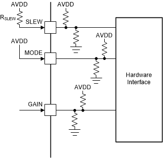
Hardware interface devices omit the four SPI pins and in their place have nSLEEP pin and three resistor-configurable inputs which are GAIN, SLEW and MODE.

Common device settings can be adjusted on the hardware interface by tying the pin logic low, logic high, or pulling up or pulling down with a resistor. Fault conditions are reported on the nFAULT pin, but detailed diagnostic information is not available.

  • The GAIN pin configures the gain of the current sense amplifier.
  • The SLEW pin configures the slew rate of the output voltage to motor.
  • The MODE pin configures the PWM control mode and OCP level.

For more information on the hardware interface, see Section 8.3.9.

Table 8-5 Hardware Pins Decode
Configuration GAIN SLEW MODE
Pin tied to AGND 0.25 V/A 35 V/us 6x PWM Mode and
9A OCP Level
Pin to 47 kΩ tied to AGND 0.5 V/A 75 V/us 6x PWM Mode and
5A OCP Level
Pin to Hi-Z 1 V/A 180 V/us 3x PWM Mode and
9A OCP Level
Pin tied to AVDD 2 V/A 230 V/us 3x PWM Mode and
5A OCP Level
Figure 8-14 DRV8311 SPI Interface
GUID-20200819-CA0I-QSVB-JJH0-DZ9GKBDDWBXV-low.gifFigure 8-15 DRV8311 Hardware Interface