ZHCSOY8B September   2021  – February 2022 DRV8311

PRODUCTION DATA  

  1. 特性
  2. 应用
  3. 说明
  4. Revision History
  5. Device Comparison Table
  6. Pin Configuration and Functions
  7. Specifications
    1. 7.1 Absolute Maximum Ratings
    2. 7.2 ESD Ratings
    3. 7.3 Recommended Operating Conditions
    4. 7.4 Thermal Information
    5. 7.5 Electrical Characteristics
    6. 7.6 SPI Timing Requirements
    7. 7.7 SPI Secondary Device Mode Timings
    8. 7.8 Typical Characteristics
  8. Detailed Description
    1. 8.1 Overview
    2. 8.2 Functional Block Diagram
    3. 8.3 Feature Description
      1. 8.3.1  Output Stage
      2. 8.3.2  Control Modes
        1. 8.3.2.1 6x PWM Mode (DRV8311S and DRV8311H variants only)
        2. 8.3.2.2 3x PWM Mode (DRV8311S and DRV8311H variants only)
        3. 8.3.2.3 PWM Generation Mode (DRV8311S and DRV8311P Variants)
      3. 8.3.3  Device Interface Modes
        1. 8.3.3.1 Serial Peripheral Interface (SPI)
        2. 8.3.3.2 Hardware Interface
      4. 8.3.4  AVDD Linear Voltage Regulator
      5. 8.3.5  Charge Pump
      6. 8.3.6  Slew Rate Control
      7. 8.3.7  Cross Conduction (Dead Time)
      8. 8.3.8  Propagation Delay
      9. 8.3.9  Pin Diagrams
        1. 8.3.9.1 Logic Level Input Pin (Internal Pulldown)
        2. 8.3.9.2 Logic Level Input Pin (Internal Pullup)
        3. 8.3.9.3 Open Drain Pin
        4. 8.3.9.4 Push Pull Pin
        5. 8.3.9.5 Four Level Input Pin
      10. 8.3.10 Current Sense Amplifiers
        1. 8.3.10.1 Current Sense Amplifier Operation
        2. 8.3.10.2 Current Sense Amplifier Offset Correction
      11. 8.3.11 Protections
        1. 8.3.11.1 VM Supply Undervoltage Lockout (NPOR)
        2. 8.3.11.2 Under Voltage Protections (UVP)
        3. 8.3.11.3 Overcurrent Protection (OCP)
          1. 8.3.11.3.1 OCP Latched Shutdown (OCP_MODE = 010b)
          2. 8.3.11.3.2 OCP Automatic Retry (OCP_MODE = 000b or 001b)
          3. 8.3.11.3.3 OCP Report Only (OCP_MODE = 011b)
          4. 8.3.11.3.4 OCP Disabled (OCP_MODE = 111b)
        4. 8.3.11.4 Thermal Protections
          1. 8.3.11.4.1 Thermal Warning (OTW)
          2. 8.3.11.4.2 Thermal Shutdown (OTSD)
    4. 8.4 Device Functional Modes
      1. 8.4.1 Functional Modes
        1. 8.4.1.1 Sleep Mode
        2. 8.4.1.2 Operating Mode
        3. 8.4.1.3 Fault Reset (CLR_FLT or nSLEEP Reset Pulse)
    5. 8.5 SPI Communication
      1. 8.5.1 Programming
        1. 8.5.1.1 SPI and tSPI Format
  9. DRV8311 Registers
  10. 10Application and Implementation
    1. 10.1 Application Information
    2. 10.2 Typical Applications
      1. 10.2.1 Three-Phase Brushless-DC Motor Control
        1. 10.2.1.1 Detailed Design Procedure
          1. 10.2.1.1.1 Motor Voltage
        2. 10.2.1.2 Driver Propagation Delay and Dead Time
        3. 10.2.1.3 Delay Compensation
        4. 10.2.1.4 Current Sensing and Output Filtering
        5. 10.2.1.5 Application Curves
    3. 10.3 Three Phase Brushless-DC tSPI Motor Control
      1. 10.3.1 Detailed Design Procedure
    4. 10.4 Alternate Applications
  11. 11Power Supply Recommendations
    1. 11.1 Bulk Capacitance
  12. 12Layout
    1. 12.1 Layout Guidelines
    2. 12.2 Layout Example
    3. 12.3 Thermal Considerations
      1. 12.3.1 Power Dissipation and Junction Temperature Estimation
  13. 13Device and Documentation Support
    1. 13.1 支持资源
    2. 13.2 Trademarks
    3. 13.3 Electrostatic Discharge Caution
    4. 13.4 术语表
  14. 14Mechanical, Packaging, and Orderable Information

封装选项

机械数据 (封装 | 引脚)
散热焊盘机械数据 (封装 | 引脚)
订购信息

Bulk Capacitance

Having an appropriate local bulk capacitance is an important factor in motor drive system design. It is generally beneficial to have more bulk capacitance, while the disadvantages are increased cost and physical size.

The amount of local capacitance needed depends on a variety of factors, including:

  • The highest current required by the motor system
  • The capacitance and current capability of the power supply
  • The amount of parasitic inductance between the power supply and motor system
  • The acceptable voltage ripple
  • The type of motor used (brushed dc, brushless DC, stepper)
  • The motor braking method

The inductance between the power supply and the motor drive system limits the rate current can change from the power supply. If the local bulk capacitance is too small, the system responds to excessive current demands or dumps from the motor with a change in voltage. When adequate bulk capacitance is used, the motor voltage remains stable and high current can be quickly supplied.

The data sheet generally provides a recommended value, but system-level testing is required to determine the appropriate sized bulk capacitor.
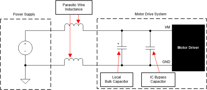
GUID-C17FA9DB-5839-448B-A584-EAD89E96E916-low.gifFigure 11-1 Example Setup of Motor Drive System With External Power Supply

The voltage rating for bulk capacitors should be higher than the operating voltage, to provide margin for cases when the motor transfers energy to the supply.