ZHCSOY8B September 2021 – February 2022 DRV8311
PRODUCTION DATA
- 1 特性
- 2 应用
- 3 说明
- 4 Revision History
- 5 Device Comparison Table
- 6 Pin Configuration and Functions
- 7 Specifications
-
8 Detailed Description
- 8.1 Overview
- 8.2 Functional Block Diagram
- 8.3
Feature Description
- 8.3.1 Output Stage
- 8.3.2 Control Modes
- 8.3.3 Device Interface Modes
- 8.3.4 AVDD Linear Voltage Regulator
- 8.3.5 Charge Pump
- 8.3.6 Slew Rate Control
- 8.3.7 Cross Conduction (Dead Time)
- 8.3.8 Propagation Delay
- 8.3.9 Pin Diagrams
- 8.3.10 Current Sense Amplifiers
- 8.3.11 Protections
- 8.4 Device Functional Modes
- 8.5 SPI Communication
- 9 DRV8311 Registers
- 10Application and Implementation
- 11Power Supply Recommendations
- 12Layout
- 13Device and Documentation Support
- 14Mechanical, Packaging, and Orderable Information
8.3.9.1 Logic Level Input Pin (Internal Pulldown)
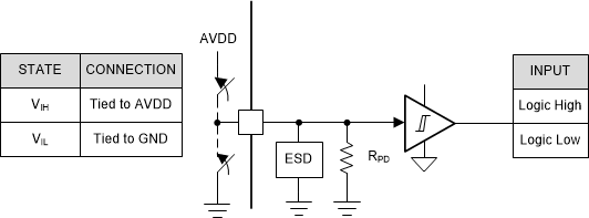
Figure 8-23 shows the input structure for the logic levels pins INHx, INLx, nSLEEP, SCLK and SDI. The input can be driven with an external resistor to GND or an external logic voltage supply. It is recommended to pull these pins low in device sleep mode to reduce leakage current through the internal pull-down resistors.
 Figure 8-23 Logic-Level Input Pin Structure