ZHCSQL7F May 2010 – May 2022 DRV8312 , DRV8332
PRODUCTION DATA
- 1 特性
- 2 应用
- 3 说明
- 4 Revision History
- 5 Pin Configuration and Functions
- 6 Specifications
- 7 Detailed Description
-
8 Application and Implementation
- 8.1 Application Information
- 8.2 Typical Applications
- 9 Power Supply Recommendations
- 10Layout
- 11Device and Documentation Support
- 12Mechanical, Packaging, and Orderable Information
7.4.1 Different Operational Modes
The DRV83x2 support two different modes of operation:
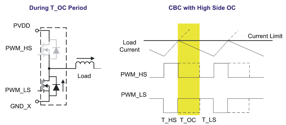
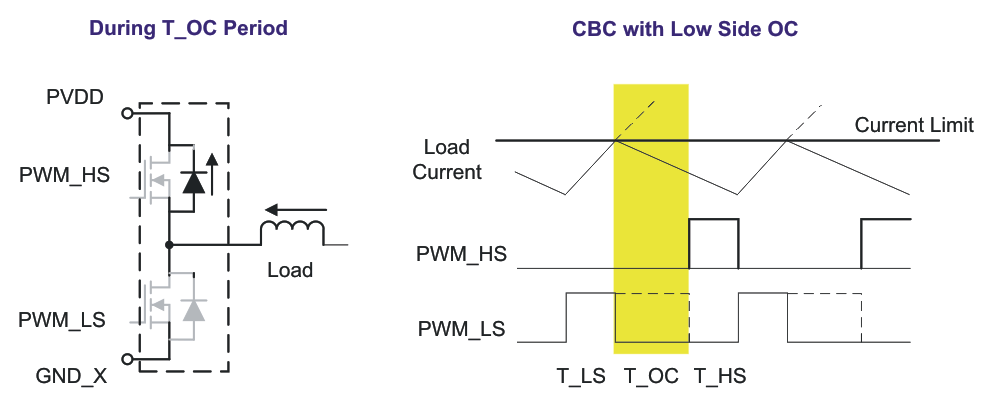
- Three-phase (3PH) or three half bridges (HB) with CBC current limit
- Three-phase or three half bridges with OC latching shutdown (no CBC current limit)
Because each half bridge has independent supply and ground pins, a shunt sensing resistor can be inserted between PVDD to PVDD_X or GND_X to GND (ground plane). A high side shunt resistor between PVDD and PVDD_X is recommended for differential current sensing because a high bias voltage on the low side sensing could affect device operation. If low side sensing has to be used, a shunt resistor value of 10 mΩ or less or sense voltage 100 mV or less is recommended.
Figure 8-1 and Figure 8-4 show the three-phase application examples, and Figure 8-5 shows how to connect to DRV83x2 with some simple logic to accommodate conventional 6 PWM inputs control.
We recommend using a complementary control scheme for switching phases to prevent circulated energy flowing inside the phases and to make current limiting feature active all the time. Complementary control scheme also forces the current flowing through sense resistors all the time to have a better current sensing and control of the system.
Figure 8-6 shows six steps trapezoidal scheme with hall sensor control and Figure 8-7 shows six steps trapezoidal scheme with sensorless control. The hall sensor sequence in real application might be different than the one we showed in Figure 8-6 depending on the motor used. Please check motor manufacture datasheet for the right sequence in applications. In six step trapezoidal complementary control scheme, a half bridge with larger than 50% duty cycle will have a positive current and a half bridge with less than 50% duty cycle will have a negative current. For normal operation, changing PWM duty cycle from 50% to 100% will adjust the current from 0 to maximum value with six steps control. It is recommended to apply a minimum 50 ns to 100 ns PWM pulse at each switching cycle at lower side to properly charge the bootstrap cap. The impact of minimum pulse at low side FET is pretty small, for example, the maximum duty cycle is 99.9% with 100 ns minimum pulse on low side. RESET_X pin can be used to get channel X into high impedance mode. If you prefer PWM switching one channel but hold low side FET of the other channel on (and third channel in Hi-Z) for 2-quadrant mode, OT latching shutdown mode is recommended to prevent the channel with low side FET on stuck in Hi-Z during OC event in CBC mode.
The DRV83x2 can also be used for sinusoidal waveform control and field oriented control. Please check TI website MCU motor control library for control algorithms.

