ZHCSQL7F May 2010 – May 2022 DRV8312 , DRV8332
PRODUCTION DATA
- 1 特性
- 2 应用
- 3 说明
- 4 Revision History
- 5 Pin Configuration and Functions
- 6 Specifications
- 7 Detailed Description
-
8 Application and Implementation
- 8.1 Application Information
- 8.2 Typical Applications
- 9 Power Supply Recommendations
- 10Layout
- 11Device and Documentation Support
- 12Mechanical, Packaging, and Orderable Information
5 Pin Configuration and Functions

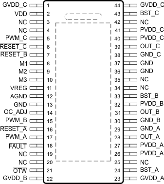
DRV8312: 44-pin
TSSOP power pad down DDW package. This package contains a thermal pad that is
located on the bottom side of the device for dissipating heat through
PCB.
Figure 5-1 DV8312HTSSOP (DDW)(Top View)
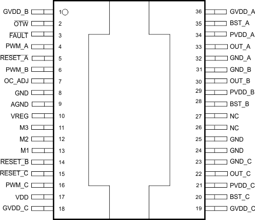
DRV8332: 36-pin
PSOP3 DKD package. This package contains a thick heat slug that is located on
the top side of the device for dissipating heat through heatsink.
Figure 5-2 DRV8332HSSOP (DKD)(Top View)Table 5-1 Pin Functions
| PIN | I/O TYPE (1) | DESCRIPTION | ||
|---|---|---|---|---|
| NAME | DRV8312 | DRV8332 | ||
| AGND | 12 | 9 | P | Analog ground |
| BST_A | 24 | 35 | P | High side bootstrap supply (BST), external capacitor to OUT_A required |
| BST_B | 33 | 28 | P | High side bootstrap supply (BST), external capacitor to OUT_B required |
| BST_C | 43 | 20 | P | High side bootstrap supply (BST), external capacitor to OUT_C required |
| GND | 13, 36, 37 | 8 | P | Ground |
| GND_A | 29 | 32 | P | Power ground for half-bridge A |
| GND_B | 30 | 31 | P | Power ground for half-bridge B |
| GND_C | 38 | 23 | P | Power ground for half-bridge C |
| GVDD_A | 23 | 36 | P | Gate-drive voltage supply |
| GVDD_B | 22 | 1 | P | Gate-drive voltage supply |
| GVDD_C | 1, 44 | 18, 19 | P | Gate-drive voltage supply |
| M1 | 8 | 13 | I | Mode selection pin |
| M2 | 9 | 12 | I | Reserved mode selection pin. AGND connection is recommended |
| M3 | 10 | 11 | I | Reserved mode selection pin, VREG connection is recommended |
| NC | 3, 4, 19, 20, 25, 34, 35, 42 | 26, 27 | - | No connection pin. Ground connection is recommended |
| OC_ADJ | 14 | 7 | O | Analog overcurrent programming pin, requires resistor to AGND |
| OTW | 21 | 2 | O | Overtemperature warning signal, open-drain, active-low. An internal pullup resistor to VREG (3.3 V) is provided on output. Level compliance for 5-V logic can be obtained by adding external pullup resistor to 5 V |
| OUT_A | 28 | 33 | O | Output, half-bridge A |
| OUT_B | 31 | 30 | O | Output, half-bridge B |
| OUT_C | 39 | 22 | O | Output, half-bridge C |
| PVDD_A | 26, 27 | 34 | P | Power supply input for half-bridge A requires close decoupling capacitor to ground. |
| PVDD_B | 32 | 29 | P | Power supply input for half-bridge B requires close decoupling capacitor to gound. |
| PVDD_C | 40, 41 | 21 | P | Power supply input for half-bridge C requires close decoupling capacitor to ground. |
| PWM_A | 17 | 4 | I | Input signal for half-bridge A |
| PWM_B | 15 | 6 | I | Input signal for half-bridge B |
| PWM_C | 5 | 16 | I | Input signal for half-bridge C |
| RESET_A | 16 | 5 | I | Reset signal for half-bridge A, active-low |
| RESET_B | 7 | 14 | I | Reset signal for half-bridge B, active-low |
| RESET_C | 6 | 15 | I | Reset signal for half-bridge C, active-low |
| FAULT | 18 | 3 | O | Fault signal, open-drain, active-low. An internal pullup resistor to VREG (3.3 V) is provided on output. Level compliance for 5-V logic can be obtained by adding external pullup resistor to 5 V |
| VDD | 2 | 17 | P | Power supply for digital voltage regulator requires capacitor to ground for decoupling. |
| VREG | 11 | 10 | P | Digital regulator supply filter pin requires 0.1-μF capacitor to AGND. |
| THERMAL PAD | -- | N/A | T | Solder the exposed thermal pad at the bottom of the DRV8312DDW package to the landing pad on the PCB. Connect the landing pad through vias to large ground plate for better thermal dissipation. |
| HEAT SLUG | N/A | -- | T | Mount heatsink with thermal interface to the heat slug on the top of the DRV8332DKD package to improve thermal dissipation. |
(1) I = input, O = output, P = power, T = thermal
Mode Selection Pins
| MODE PINS | DESCRIPTION | ||
|---|---|---|---|
| M3 | M2 | M1 | |
| 1 | 0 | 0 | Three-phase or three half bridges with cycle-by-cycle current limit |
| 1 | 0 | 1 | Three-phase or three half bridges with OC latching shutdown (no cycle-by-cycle current limit) |
| 0 | x | x | Reserved |