ZHCSR87 December   2022 DRV8316C

PRODUCTION DATA  

  1. 特性
  2. 应用
  3. 说明
  4. Revision History
  5. Device Comparison Table
  6. Pin Configuration and Functions
  7. Specifications
    1. 7.1 Absolute Maximum Ratings
    2. 7.2 ESD Ratings
    3. 7.3 Recommended Operating Conditions
    4. 7.4 Thermal Information
    5. 7.5 Electrical Characteristics
    6. 7.6 SPI Timing Requirements
    7. 7.7 SPI Slave Mode Timings
    8. 7.8 Typical Characteristics
  8. Detailed Description
    1. 8.1 Overview
    2. 8.2 Functional Block Diagram
    3. 8.3 Feature Description
      1. 8.3.1  Output Stage
      2. 8.3.2  Control Modes
        1. 8.3.2.1 6x PWM Mode (PWM_MODE = 00b or MODE Pin Tied to AGND)
        2. 8.3.2.2 3x PWM Mode (PWM_MODE = 10b or MODE Pin is Connected to AVDD with RMODE)
        3. 8.3.2.3 Current Limit Mode (PWM_MODE = 01b / 11b or MODE Pin is Hi-Z or Connected to AVDD)
      3. 8.3.3  Device Interface Modes
        1. 8.3.3.1 Serial Peripheral Interface (SPI)
        2. 8.3.3.2 Hardware Interface
      4. 8.3.4  Step-Down Mixed-Mode Buck Regulator
        1. 8.3.4.1 Buck in Inductor Mode
        2. 8.3.4.2 Buck in Resistor mode
        3. 8.3.4.3 Buck Regulator with External LDO
        4. 8.3.4.4 AVDD Power Sequencing on Buck Regulator
        5. 8.3.4.5 Mixed mode Buck Operation and Control
      5. 8.3.5  AVDD Linear Voltage Regulator
      6. 8.3.6  Charge Pump
      7. 8.3.7  Slew Rate Control
      8. 8.3.8  Cross Conduction (Dead Time)
      9. 8.3.9  Propagation Delay
        1. 8.3.9.1 Driver Delay Compensation
      10. 8.3.10 Pin Diagrams
        1. 8.3.10.1 Logic Level Input Pin (Internal Pulldown)
        2. 8.3.10.2 Logic Level Input Pin (Internal Pullup)
        3. 8.3.10.3 Open Drain Pin
        4. 8.3.10.4 Push Pull Pin
        5. 8.3.10.5 Four Level Input Pin
      11. 8.3.11 Current Sense Amplifiers
        1. 8.3.11.1 Current Sense Amplifier Operation
      12. 8.3.12 Active Demagnetization
        1. 8.3.12.1 Automatic Synchronous Rectification Mode (ASR Mode)
          1. 8.3.12.1.1 Automatic Synchronous Rectification in Commutation
          2. 8.3.12.1.2 Automatic Synchronous Rectification in PWM Mode
        2. 8.3.12.2 Automatic Asynchronous Rectification Mode (AAR Mode)
      13. 8.3.13 Cycle-by-Cycle Current Limit
        1. 8.3.13.1 Cycle by Cycle Current Limit with 100% Duty Cycle Input
      14. 8.3.14 Protections
        1. 8.3.14.1 VM Supply Undervoltage Lockout (NPOR)
        2. 8.3.14.2 AVDD Undervoltage Lockout (AVDD_UV)
        3. 8.3.14.3 BUCK Undervoltage Lockout (BUCK_UV)
        4. 8.3.14.4 VCP Charge Pump Undervoltage Lockout (CPUV)
        5. 8.3.14.5 Overvoltage Protection (OVP)
        6. 8.3.14.6 Overcurrent Protection (OCP)
          1. 8.3.14.6.1 OCP Latched Shutdown (OCP_MODE = 00b)
          2. 8.3.14.6.2 OCP Automatic Retry (OCP_MODE = 01b)
          3. 8.3.14.6.3 OCP Report Only (OCP_MODE = 10b)
          4. 8.3.14.6.4 OCP Disabled (OCP_MODE = 11b)
        7. 8.3.14.7 Buck Overcurrent Protection
        8. 8.3.14.8 Thermal Warning (OTW)
        9. 8.3.14.9 Thermal Shutdown (OTS)
          1. 8.3.14.9.1 OTS FET
          2. 8.3.14.9.2 OTS (Non FET)
    4. 8.4 Device Functional Modes
      1. 8.4.1 Functional Modes
        1. 8.4.1.1 Sleep Mode
        2. 8.4.1.2 Operating Mode
        3. 8.4.1.3 Fault Reset (CLR_FLT or nSLEEP Reset Pulse)
      2. 8.4.2 DRVOFF functionality
    5. 8.5 SPI Communication
      1. 8.5.1 Programming
        1. 8.5.1.1 SPI Format
    6. 8.6 Register Map
      1. 8.6.1 STATUS Registers
      2. 8.6.2 CONTROL Registers
  9. Application and Implementation
    1. 9.1 Application Information
    2. 9.2 Typical Applications
      1. 9.2.1 Three-Phase Brushless-DC Motor Control
        1. 9.2.1.1 Detailed Design Procedure
          1. 9.2.1.1.1 Motor Voltage
          2. 9.2.1.1.2 Using Active Demagnetization
          3. 9.2.1.1.3 Driver Propagation Delay and Dead Time
          4. 9.2.1.1.4 Using Delay Compensation
          5. 9.2.1.1.5 Using the Buck Regulator
          6. 9.2.1.1.6 Current Sensing and Output Filtering
        2. 9.2.1.2 Application Curves
      2. 9.2.2 Three-Phase Brushless-DC Motor Control With Current Limit
        1. 9.2.2.1 Block Diagram
        2. 9.2.2.2 Detailed Design Procedure
          1. 9.2.2.2.1 Motor Voltage
          2. 9.2.2.2.2 ILIM Implementation
        3. 9.2.2.3 Application Curves
      3. 9.2.3 Brushed-DC and Solenoid Load
        1. 9.2.3.1 Block Diagram
        2. 9.2.3.2 Design Requirements
          1. 9.2.3.2.1 Detailed Design Procedure
      4. 9.2.4 Three Solenoid Loads
        1. 9.2.4.1 Block Diagram
        2. 9.2.4.2 Design Requirements
          1. 9.2.4.2.1 Detailed Design Procedure
  10. 10Power Supply Recommendations
    1. 10.1 Bulk Capacitance
  11. 11Layout
    1. 11.1 Layout Guidelines
    2. 11.2 Layout Example
    3. 11.3 Thermal Considerations
      1. 11.3.1 Power Dissipation
  12. 12Device and Documentation Support
    1. 12.1 Documentation Support
      1. 12.1.1 Related Documentation
    2. 12.2 支持资源
    3. 12.3 Trademarks
    4. 12.4 Electrostatic Discharge Caution
    5. 12.5 术语表
  13. 13Mechanical, Packaging, and Orderable Information

封装选项

机械数据 (封装 | 引脚)
散热焊盘机械数据 (封装 | 引脚)
订购信息

SPI Format

The SDI input data word is 16 bits long and consists of the following format:

  • 1 read or write bit, W (bit B15)
  • 6 address bits, A (bits B14 through B9)
  • Parity bit, P (bit B8). Parity bit is set such that the SDI input data word has even number of 1s and 0s
  • 8 data bits, D (bits B7 through B0)

The SDO output data word is 16 bits long and the first 8 bits are status bits. The data word is the content of the register being accessed.

For a write command (W0 = 0), the response word on the SDO pin is the data currently in the register being written to.

For a read command (W0 = 1), the response word is the data currently in the register being read.

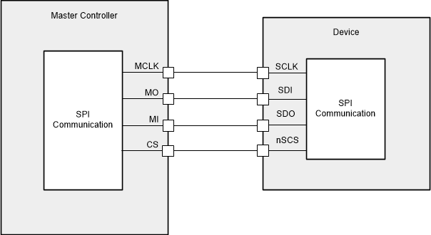
GUID-45CFFFCC-0228-463C-9D43-760E13CCA108-low.gifFigure 8-45
GUID-20210104-CA0I-NW6R-RRRC-NN1F9VZZ3Z5N-low.gif Figure 8-46
Table 8-9 SDI Input Data Word Format
R/WADDRESSParityDATA
B15B14B13B12B11B10B9B8B7B6B5B4B3B2B1B0
W0A5A4A3A2A1A0PD7D6D5D4D3D2D1D0
Table 8-10 SDO Output Data Word Format
STATUSDATA
B15B14B13B12B11B10B9B8B7B6B5B4B3B2B1B0
S7S6S5S4S3S2S1S0D7D6D5D4D3D2D1D0
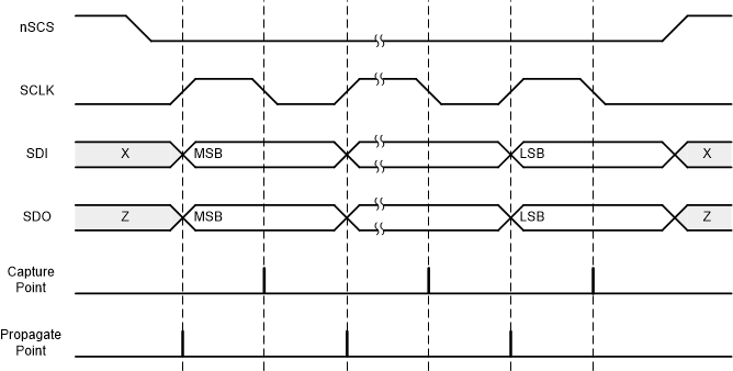
GUID-ADDBDEF1-0CF8-477E-8890-478E37613453-low.gifFigure 8-47 SPI Secondary Timing Diagram

SPI Error Handling

SPI Frame Error (SPI_SCLK_FLT: If the nSCS gets deasserted before the end of 16-bit frame, SPI frame error is detected and SPI_SCLK_FLT bit is set in STAT2. The SPI_SCLK_FLT status bit is latched and can be cleared when a clear faults command is issued either through the CLR_FLT bit or an nSLEEP reset pulse

SPI Address Error (SPI_ADDR_FLT): If an invalid address is provided in the ADDR field of the input SPI data on SDI, SPI address error is detected and SPI_ADDR_FLT bit in STAT2 is set. Invalid address is any address that is not defined in Section 8.6 i.e. address not falling in the range of address 0x0 to 0xC. The SPI_ADDR_FLT status bit is latched and can be cleared when a clear faults command is issued either through the CLR_FLT bit or an nSLEEP reset pulse