ZHCSG01C
February 2017 – August 2018
DRV8320
,
DRV8320R
,
DRV8323
,
DRV8323R
PRODUCTION DATA.
1
特性
2
应用
3
说明
简化原理图
4
修订历史记录
5
Device Comparison Table
6
Pin Configuration and Functions
Pin Functions—32-Pin DRV8320 Devices
Pin Functions—40-Pin DRV8320R Devices
Pin Functions—40-Pin DRV8323 Devices
Pin Functions—48-Pin DRV8323R Devices
7
Specifications
7.1
Absolute Maximum Ratings
7.2
ESD Ratings
7.3
Recommended Operating Conditions
7.4
Thermal Information
7.5
Electrical Characteristics
7.6
SPI Timing Requirements
7.7
Typical Characteristics
8
Detailed Description
8.1
Overview
8.2
Functional Block Diagram
8.3
Feature Description
8.3.1
Three Phase Smart Gate Drivers
8.3.1.1
PWM Control Modes
8.3.1.1.1
6x PWM Mode (PWM_MODE = 00b or MODE Pin Tied to AGND)
8.3.1.1.2
3x PWM Mode (PWM_MODE = 01b or MODE Pin = 47 kΩ to AGND)
8.3.1.1.3
1x PWM Mode (PWM_MODE = 10b or MODE Pin = Hi-Z)
8.3.1.1.4
Independent PWM Mode (PWM_MODE = 11b or MODE Pin Tied to DVDD)
8.3.1.2
Device Interface Modes
8.3.1.2.1
Serial Peripheral Interface (SPI)
8.3.1.2.2
Hardware Interface
8.3.1.3
Gate Driver Voltage Supplies
8.3.1.4
Smart Gate Drive Architecture
8.3.1.4.1
IDRIVE: MOSFET Slew-Rate Control
8.3.1.4.2
TDRIVE: MOSFET Gate Drive Control
8.3.1.4.3
Propagation Delay
8.3.1.4.4
MOSFET VDS Monitors
8.3.1.4.5
VDRAIN Sense Pin
8.3.2
DVDD Linear Voltage Regulator
8.3.3
Pin Diagrams
8.3.4
Low-Side Current Sense Amplifiers (DRV8323 and DRV8323R Only)
8.3.4.1
Bidirectional Current Sense Operation
8.3.4.2
Unidirectional Current Sense Operation (SPI only)
8.3.4.3
Auto Offset Calibration
8.3.4.4
MOSFET VDS Sense Mode (SPI Only)
8.3.5
Step-Down Buck Regulator
8.3.5.1
Fixed Frequency PWM Control
8.3.5.2
Bootstrap Voltage (CB)
8.3.5.3
Output Voltage Setting
8.3.5.4
Enable nSHDN and VIN Undervoltage Lockout
8.3.5.5
Current Limit
8.3.5.6
Overvoltage Transient Protection
8.3.5.7
Thermal Shutdown
8.3.6
Gate Driver Protective Circuits
8.3.6.1
VM Supply Undervoltage Lockout (UVLO)
8.3.6.2
VCP Charge Pump Undervoltage Lockout (CPUV)
8.3.6.3
MOSFET VDS Overcurrent Protection (VDS_OCP)
8.3.6.3.1
VDS Latched Shutdown (OCP_MODE = 00b)
8.3.6.3.2
VDS Automatic Retry (OCP_MODE = 01b)
8.3.6.3.3
VDS Report Only (OCP_MODE = 10b)
8.3.6.3.4
VDS Disabled (OCP_MODE = 11b)
8.3.6.4
VSENSE Overcurrent Protection (SEN_OCP)
8.3.6.4.1
VSENSE Latched Shutdown (OCP_MODE = 00b)
8.3.6.4.2
VSENSE Automatic Retry (OCP_MODE = 01b)
8.3.6.4.3
VSENSE Report Only (OCP_MODE = 10b)
8.3.6.4.4
VSENSE Disabled (OCP_MODE = 11b or DIS_SEN = 1b)
8.3.6.5
Gate Driver Fault (GDF)
8.3.6.6
Thermal Warning (OTW)
8.3.6.7
Thermal Shutdown (OTSD)
8.4
Device Functional Modes
8.4.1
Gate Driver Functional Modes
8.4.1.1
Sleep Mode
8.4.1.2
Operating Mode
8.4.1.3
Fault Reset (CLR_FLT or ENABLE Reset Pulse)
8.4.2
Buck Regulator Functional Modes
8.4.2.1
Continuous Conduction Mode (CCM)
8.4.2.2
Eco-mode Control Scheme
8.5
Programming
8.5.1
SPI Communication
8.5.1.1
SPI
8.5.1.1.1
SPI Format
8.6
Register Maps
Table 1.
DRV832xS and DRV832xRS Register Map
8.6.1
Status Registers
8.6.1.1
Fault Status Register 1 (address = 0x00)
Table 11.
Fault Status Register 1 Field Descriptions
8.6.1.2
Fault Status Register 2 (address = 0x01)
Table 12.
Fault Status Register 2 Field Descriptions
8.6.2
Control Registers
8.6.2.1
Driver Control Register (address = 0x02)
Table 14.
Driver Control Field Descriptions
8.6.2.2
Gate Drive HS Register (address = 0x03)
Table 15.
Gate Drive HS Field Descriptions
8.6.2.3
Gate Drive LS Register (address = 0x04)
Table 16.
Gate Drive LS Register Field Descriptions
8.6.2.4
OCP Control Register (address = 0x05)
Table 17.
OCP Control Field Descriptions
8.6.2.5
CSA Control Register (DRV8323x Only) (address = 0x06)
Table 18.
CSA Control Field Descriptions
9
Application and Implementation
9.1
Application Information
9.2
Typical Application
9.2.1
Primary Application
9.2.1.1
Design Requirements
9.2.1.2
Detailed Design Procedure
9.2.1.2.1
External MOSFET Support
9.2.1.2.1.1
Example
9.2.1.2.2
IDRIVE Configuration
9.2.1.2.2.1
Example
9.2.1.2.3
VDS Overcurrent Monitor Configuration
9.2.1.2.3.1
Example
9.2.1.2.4
Sense Amplifier Bidirectional Configuration (DRV8323 and DRV8323R)
9.2.1.2.4.1
Example
9.2.1.2.5
Buck Regulator Configuration (DRV8320R and DRV8323R)
9.2.1.3
Application Curves
9.2.2
Alternative Application
9.2.2.1
Design Requirements
9.2.2.2
Detailed Design Procedure
9.2.2.2.1
Sense Amplifier Unidirectional Configuration
9.2.2.2.1.1
Example
10
Power Supply Recommendations
10.1
Bulk Capacitance Sizing
11
Layout
11.1
Layout Guidelines
11.1.1
Buck-Regulator Layout Guidelines
11.2
Layout Example
12
器件和文档支持
12.1
器件支持
12.1.1
器件命名规则
12.2
文档支持
12.2.1
相关文档
12.3
相关链接
12.4
接收文档更新通知
12.5
社区资源
12.6
商标
12.7
静电放电警告
12.8
术语表
13
机械、封装和可订购信息
封装选项
机械数据 (封装 | 引脚)
RHA|40
MPQF135D
散热焊盘机械数据 (封装 | 引脚)
订购信息
zhcsg01c_oa
zhcsg01c_pm
9.2.1.3
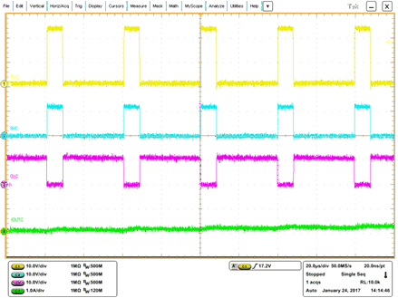
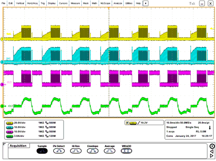
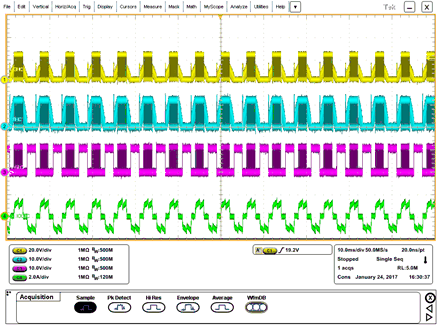
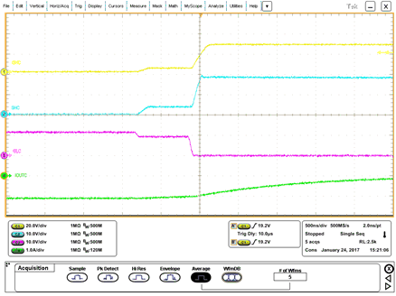
Application Curves
Figure 52.
Gate Drive at 20% Duty Cycle
Figure 54.
BLDC Motor Commutation 1000 RPM
Figure 56.
IDRIVE Maximum Setting Positive Current
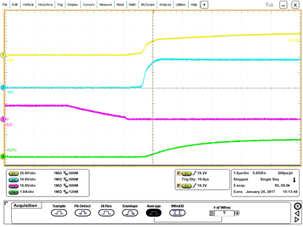
Figure 58.
IDRIVE Minimum Setting Positive Current
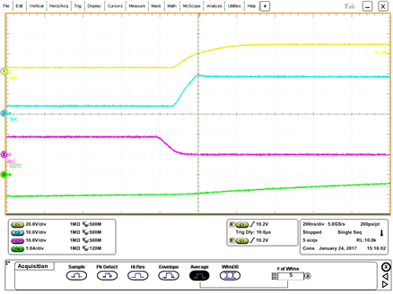
Figure 60.
IDRIVE 260 to 520-mA Setting Negative Current
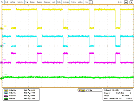
Figure 53.
Gate Drive at 80% Duty Cycle
Figure 55.
BLDC Motor Commutation 2000 RPM
Figure 57.
IDRIVE Maximum Setting Negative Current
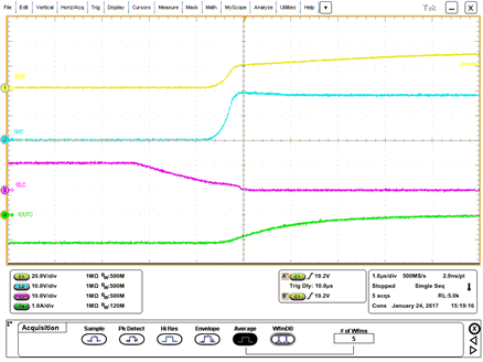
Figure 59.
IDRIVE Minimum Setting Negative Current
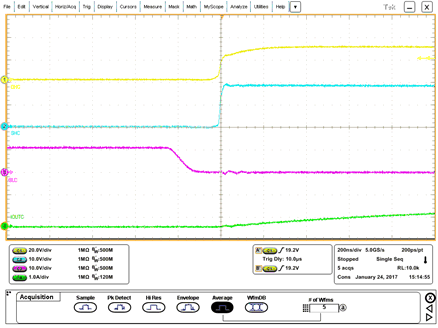
Figure 61.
IDRIVE 260 to 520-mA Setting Positive Current
千亿体育app官网登录(中国)官方网站IOS/安卓通用版/手机APP
|
米乐app下载官网(中国)|ios|Android/通用版APP最新版
|
米乐|米乐·M6(中国大陆)官方网站
|
千亿体育登陆地址
|
华体会体育(中国)HTH·官方网站
|
千赢qy国际_全站最新版千赢qy国际V6.2.14安卓/IOS下载
|
18新利网v1.2.5|中国官方网站
|
bob电竞真人(中国官网)安卓/ios苹果/电脑版【1.97.95版下载】
|
千亿体育app官方下载(中国)官方网站IOS/安卓/手机APP下载安装
|