ZHCSG01C February   2017  – August 2018 DRV8320 , DRV8320R , DRV8323 , DRV8323R

PRODUCTION DATA.  

  1. 特性
  2. 应用
  3. 说明
    1.     简化原理图
  4. 修订历史记录
  5. Device Comparison Table
  6. Pin Configuration and Functions
    1.     Pin Functions—32-Pin DRV8320 Devices
    2.     Pin Functions—40-Pin DRV8320R Devices
    3.     Pin Functions—40-Pin DRV8323 Devices
    4.     Pin Functions—48-Pin DRV8323R Devices
  7. Specifications
    1. 7.1 Absolute Maximum Ratings
    2. 7.2 ESD Ratings
    3. 7.3 Recommended Operating Conditions
    4. 7.4 Thermal Information
    5. 7.5 Electrical Characteristics
    6. 7.6 SPI Timing Requirements
    7. 7.7 Typical Characteristics
  8. Detailed Description
    1. 8.1 Overview
    2. 8.2 Functional Block Diagram
    3. 8.3 Feature Description
      1. 8.3.1 Three Phase Smart Gate Drivers
        1. 8.3.1.1 PWM Control Modes
          1. 8.3.1.1.1 6x PWM Mode (PWM_MODE = 00b or MODE Pin Tied to AGND)
          2. 8.3.1.1.2 3x PWM Mode (PWM_MODE = 01b or MODE Pin = 47 kΩ to AGND)
          3. 8.3.1.1.3 1x PWM Mode (PWM_MODE = 10b or MODE Pin = Hi-Z)
          4. 8.3.1.1.4 Independent PWM Mode (PWM_MODE = 11b or MODE Pin Tied to DVDD)
        2. 8.3.1.2 Device Interface Modes
          1. 8.3.1.2.1 Serial Peripheral Interface (SPI)
          2. 8.3.1.2.2 Hardware Interface
        3. 8.3.1.3 Gate Driver Voltage Supplies
        4. 8.3.1.4 Smart Gate Drive Architecture
          1. 8.3.1.4.1 IDRIVE: MOSFET Slew-Rate Control
          2. 8.3.1.4.2 TDRIVE: MOSFET Gate Drive Control
          3. 8.3.1.4.3 Propagation Delay
          4. 8.3.1.4.4 MOSFET VDS Monitors
          5. 8.3.1.4.5 VDRAIN Sense Pin
      2. 8.3.2 DVDD Linear Voltage Regulator
      3. 8.3.3 Pin Diagrams
      4. 8.3.4 Low-Side Current Sense Amplifiers (DRV8323 and DRV8323R Only)
        1. 8.3.4.1 Bidirectional Current Sense Operation
        2. 8.3.4.2 Unidirectional Current Sense Operation (SPI only)
        3. 8.3.4.3 Auto Offset Calibration
        4. 8.3.4.4 MOSFET VDS Sense Mode (SPI Only)
      5. 8.3.5 Step-Down Buck Regulator
        1. 8.3.5.1 Fixed Frequency PWM Control
        2. 8.3.5.2 Bootstrap Voltage (CB)
        3. 8.3.5.3 Output Voltage Setting
        4. 8.3.5.4 Enable nSHDN and VIN Undervoltage Lockout
        5. 8.3.5.5 Current Limit
        6. 8.3.5.6 Overvoltage Transient Protection
        7. 8.3.5.7 Thermal Shutdown
      6. 8.3.6 Gate Driver Protective Circuits
        1. 8.3.6.1 VM Supply Undervoltage Lockout (UVLO)
        2. 8.3.6.2 VCP Charge Pump Undervoltage Lockout (CPUV)
        3. 8.3.6.3 MOSFET VDS Overcurrent Protection (VDS_OCP)
          1. 8.3.6.3.1 VDS Latched Shutdown (OCP_MODE = 00b)
          2. 8.3.6.3.2 VDS Automatic Retry (OCP_MODE = 01b)
          3. 8.3.6.3.3 VDS Report Only (OCP_MODE = 10b)
          4. 8.3.6.3.4 VDS Disabled (OCP_MODE = 11b)
        4. 8.3.6.4 VSENSE Overcurrent Protection (SEN_OCP)
          1. 8.3.6.4.1 VSENSE Latched Shutdown (OCP_MODE = 00b)
          2. 8.3.6.4.2 VSENSE Automatic Retry (OCP_MODE = 01b)
          3. 8.3.6.4.3 VSENSE Report Only (OCP_MODE = 10b)
          4. 8.3.6.4.4 VSENSE Disabled (OCP_MODE = 11b or DIS_SEN = 1b)
        5. 8.3.6.5 Gate Driver Fault (GDF)
        6. 8.3.6.6 Thermal Warning (OTW)
        7. 8.3.6.7 Thermal Shutdown (OTSD)
    4. 8.4 Device Functional Modes
      1. 8.4.1 Gate Driver Functional Modes
        1. 8.4.1.1 Sleep Mode
        2. 8.4.1.2 Operating Mode
        3. 8.4.1.3 Fault Reset (CLR_FLT or ENABLE Reset Pulse)
      2. 8.4.2 Buck Regulator Functional Modes
        1. 8.4.2.1 Continuous Conduction Mode (CCM)
        2. 8.4.2.2 Eco-mode Control Scheme
    5. 8.5 Programming
      1. 8.5.1 SPI Communication
        1. 8.5.1.1 SPI
          1. 8.5.1.1.1 SPI Format
    6. 8.6 Register Maps
      1. Table 1. DRV832xS and DRV832xRS Register Map
      2. 8.6.1    Status Registers
        1. 8.6.1.1 Fault Status Register 1 (address = 0x00)
          1. Table 11. Fault Status Register 1 Field Descriptions
        2. 8.6.1.2 Fault Status Register 2 (address = 0x01)
          1. Table 12. Fault Status Register 2 Field Descriptions
      3. 8.6.2    Control Registers
        1. 8.6.2.1 Driver Control Register (address = 0x02)
          1. Table 14. Driver Control Field Descriptions
        2. 8.6.2.2 Gate Drive HS Register (address = 0x03)
          1. Table 15. Gate Drive HS Field Descriptions
        3. 8.6.2.3 Gate Drive LS Register (address = 0x04)
          1. Table 16. Gate Drive LS Register Field Descriptions
        4. 8.6.2.4 OCP Control Register (address = 0x05)
          1. Table 17. OCP Control Field Descriptions
        5. 8.6.2.5 CSA Control Register (DRV8323x Only) (address = 0x06)
          1. Table 18. CSA Control Field Descriptions
  9. Application and Implementation
    1. 9.1 Application Information
    2. 9.2 Typical Application
      1. 9.2.1 Primary Application
        1. 9.2.1.1 Design Requirements
        2. 9.2.1.2 Detailed Design Procedure
          1. 9.2.1.2.1 External MOSFET Support
            1. 9.2.1.2.1.1 Example
          2. 9.2.1.2.2 IDRIVE Configuration
            1. 9.2.1.2.2.1 Example
          3. 9.2.1.2.3 VDS Overcurrent Monitor Configuration
            1. 9.2.1.2.3.1 Example
          4. 9.2.1.2.4 Sense Amplifier Bidirectional Configuration (DRV8323 and DRV8323R)
            1. 9.2.1.2.4.1 Example
          5. 9.2.1.2.5 Buck Regulator Configuration (DRV8320R and DRV8323R)
        3. 9.2.1.3 Application Curves
      2. 9.2.2 Alternative Application
        1. 9.2.2.1 Design Requirements
        2. 9.2.2.2 Detailed Design Procedure
          1. 9.2.2.2.1 Sense Amplifier Unidirectional Configuration
            1. 9.2.2.2.1.1 Example
  10. 10Power Supply Recommendations
    1. 10.1 Bulk Capacitance Sizing
  11. 11Layout
    1. 11.1 Layout Guidelines
      1. 11.1.1 Buck-Regulator Layout Guidelines
    2. 11.2 Layout Example
  12. 12器件和文档支持
    1. 12.1 器件支持
      1. 12.1.1 器件命名规则
    2. 12.2 文档支持
      1. 12.2.1 相关文档
    3. 12.3 相关链接
    4. 12.4 接收文档更新通知
    5. 12.5 社区资源
    6. 12.6 商标
    7. 12.7 静电放电警告
    8. 12.8 术语表
  13. 13机械、封装和可订购信息

封装选项

机械数据 (封装 | 引脚)
散热焊盘机械数据 (封装 | 引脚)
订购信息

Independent PWM Mode (PWM_MODE = 11b or MODE Pin Tied to DVDD)

In independent PWM mode, the corresponding input pin independently controls each high-side and low-side gate driver. This control mode lets the DRV832x family of devices drive separate high-side and low-side loads with each half-bridge. These types of loads include unidirectional brushed DC motors, solenoids, and low-side and high-side switches. In this mode, if the system is configured in a half-bridge configuration, turning on both the high-side and low-side MOSFETs at the same time causes shoot-through.

Table 6. Independent PWM Mode Truth Table

INLx INHx GLx GHx
0 0 L L
0 1 L H
1 0 H L
1 1 H H

Because the high-side and low-side VDS overcurrent monitors share the SHx sense line, using the monitors when both the high-side and low-side gate drivers of one half-bridge are split and being used is not possible. In this case, connect the SHx pin to the high-side driver and disable the VDS overcurrent monitors as shown in Figure 20.
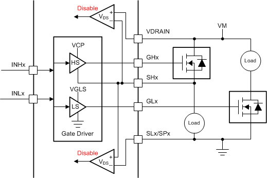
DRV8320 DRV8320R DRV8323 DRV8323R drv832xx-independent-pwm-both.gifFigure 20. Independent PWM High-Side and Low-Side Drivers

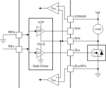
If the half-bridge is used to implement only a high-side or low-side driver, using the VDS overcurrent monitors is still possible. Connect the SHx pin as shown in Figure 21 or Figure 22. The unused gate driver and the corresponding input can stay disconnected.
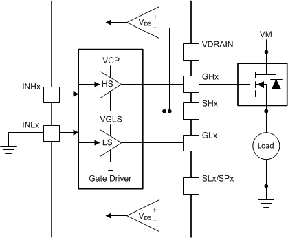
DRV8320 DRV8320R DRV8323 DRV8323R drv832xx-independent-pwm-hs.gifFigure 21. One High-Side Driver
DRV8320 DRV8320R DRV8323 DRV8323R drv832xx-independent-pwm-ls.gifFigure 22. One Low-Side Driver