ZHCSG01C February 2017 – August 2018 DRV8320 , DRV8320R , DRV8323 , DRV8323R
PRODUCTION DATA.
- 1 特性
- 2 应用
- 3 说明
- 4 修订历史记录
- 5 Device Comparison Table
- 6 Pin Configuration and Functions
- 7 Specifications
-
8 Detailed Description
- 8.1 Overview
- 8.2 Functional Block Diagram
- 8.3
Feature Description
- 8.3.1 Three Phase Smart Gate Drivers
- 8.3.2 DVDD Linear Voltage Regulator
- 8.3.3 Pin Diagrams
- 8.3.4 Low-Side Current Sense Amplifiers (DRV8323 and DRV8323R Only)
- 8.3.5 Step-Down Buck Regulator
- 8.3.6 Gate Driver Protective Circuits
- 8.4 Device Functional Modes
- 8.5 Programming
- 8.6
Register Maps
- Table 1. DRV832xS and DRV832xRS Register Map
- 8.6.1 Status Registers
- 8.6.2 Control Registers
-
9 Application and Implementation
- 9.1 Application Information
- 9.2
Typical Application
- 9.2.1
Primary Application
- 9.2.1.1 Design Requirements
- 9.2.1.2 Detailed Design Procedure
- 9.2.1.3 Application Curves
- 9.2.2 Alternative Application
- 9.2.1
Primary Application
- 10Power Supply Recommendations
- 11Layout
- 12器件和文档支持
- 13机械、封装和可订购信息
8.3.1.3 Gate Driver Voltage Supplies
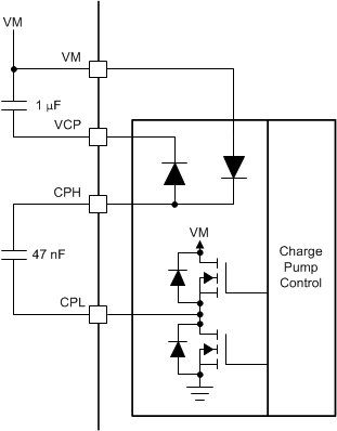
The voltage supply for the high-side gate driver is created using a doubler charge pump that operates from the VM voltage supply input. The charge pump lets the gate driver correctly bias the high-side MOSFET gate with respect to the source across a wide input supply voltage range. The charge pump is regulated to keep a fixed output voltage of VVM + 11 V and supports an average output current of 25 mA. When VVM is less than 12 V, the charge pump operates in full doubler mode and generates VVCP = 2 × VVM – 1.5 V when unloaded. The charge pump is continuously monitored for undervoltage events to prevent under-driven MOSFET conditions. The charge pump requires a X5R or X7R, 1-µF, 16-V ceramic capacitor between the VM and VCP pins to act as the storage capacitor. Additionally, a X5R or X7R, 47-nF, VM-rated ceramic capacitor is required between the CPH and CPL pins to act as the flying capacitor.
 Figure 25. Charge Pump Architecture
 The voltage supply of the low-side gate driver is created using a linear regulator that operates from the VM voltage supply input. The linear regulator lets the gate driver correctly bias the low-side MOSFET gate with respect to ground. The linear regulator output is fixed at 11 V and supports an output current of 25 mA.