ZHCSG01C February   2017  – August 2018 DRV8320 , DRV8320R , DRV8323 , DRV8323R

PRODUCTION DATA.  

  1. 特性
  2. 应用
  3. 说明
    1.     简化原理图
  4. 修订历史记录
  5. Device Comparison Table
  6. Pin Configuration and Functions
    1.     Pin Functions—32-Pin DRV8320 Devices
    2.     Pin Functions—40-Pin DRV8320R Devices
    3.     Pin Functions—40-Pin DRV8323 Devices
    4.     Pin Functions—48-Pin DRV8323R Devices
  7. Specifications
    1. 7.1 Absolute Maximum Ratings
    2. 7.2 ESD Ratings
    3. 7.3 Recommended Operating Conditions
    4. 7.4 Thermal Information
    5. 7.5 Electrical Characteristics
    6. 7.6 SPI Timing Requirements
    7. 7.7 Typical Characteristics
  8. Detailed Description
    1. 8.1 Overview
    2. 8.2 Functional Block Diagram
    3. 8.3 Feature Description
      1. 8.3.1 Three Phase Smart Gate Drivers
        1. 8.3.1.1 PWM Control Modes
          1. 8.3.1.1.1 6x PWM Mode (PWM_MODE = 00b or MODE Pin Tied to AGND)
          2. 8.3.1.1.2 3x PWM Mode (PWM_MODE = 01b or MODE Pin = 47 kΩ to AGND)
          3. 8.3.1.1.3 1x PWM Mode (PWM_MODE = 10b or MODE Pin = Hi-Z)
          4. 8.3.1.1.4 Independent PWM Mode (PWM_MODE = 11b or MODE Pin Tied to DVDD)
        2. 8.3.1.2 Device Interface Modes
          1. 8.3.1.2.1 Serial Peripheral Interface (SPI)
          2. 8.3.1.2.2 Hardware Interface
        3. 8.3.1.3 Gate Driver Voltage Supplies
        4. 8.3.1.4 Smart Gate Drive Architecture
          1. 8.3.1.4.1 IDRIVE: MOSFET Slew-Rate Control
          2. 8.3.1.4.2 TDRIVE: MOSFET Gate Drive Control
          3. 8.3.1.4.3 Propagation Delay
          4. 8.3.1.4.4 MOSFET VDS Monitors
          5. 8.3.1.4.5 VDRAIN Sense Pin
      2. 8.3.2 DVDD Linear Voltage Regulator
      3. 8.3.3 Pin Diagrams
      4. 8.3.4 Low-Side Current Sense Amplifiers (DRV8323 and DRV8323R Only)
        1. 8.3.4.1 Bidirectional Current Sense Operation
        2. 8.3.4.2 Unidirectional Current Sense Operation (SPI only)
        3. 8.3.4.3 Auto Offset Calibration
        4. 8.3.4.4 MOSFET VDS Sense Mode (SPI Only)
      5. 8.3.5 Step-Down Buck Regulator
        1. 8.3.5.1 Fixed Frequency PWM Control
        2. 8.3.5.2 Bootstrap Voltage (CB)
        3. 8.3.5.3 Output Voltage Setting
        4. 8.3.5.4 Enable nSHDN and VIN Undervoltage Lockout
        5. 8.3.5.5 Current Limit
        6. 8.3.5.6 Overvoltage Transient Protection
        7. 8.3.5.7 Thermal Shutdown
      6. 8.3.6 Gate Driver Protective Circuits
        1. 8.3.6.1 VM Supply Undervoltage Lockout (UVLO)
        2. 8.3.6.2 VCP Charge Pump Undervoltage Lockout (CPUV)
        3. 8.3.6.3 MOSFET VDS Overcurrent Protection (VDS_OCP)
          1. 8.3.6.3.1 VDS Latched Shutdown (OCP_MODE = 00b)
          2. 8.3.6.3.2 VDS Automatic Retry (OCP_MODE = 01b)
          3. 8.3.6.3.3 VDS Report Only (OCP_MODE = 10b)
          4. 8.3.6.3.4 VDS Disabled (OCP_MODE = 11b)
        4. 8.3.6.4 VSENSE Overcurrent Protection (SEN_OCP)
          1. 8.3.6.4.1 VSENSE Latched Shutdown (OCP_MODE = 00b)
          2. 8.3.6.4.2 VSENSE Automatic Retry (OCP_MODE = 01b)
          3. 8.3.6.4.3 VSENSE Report Only (OCP_MODE = 10b)
          4. 8.3.6.4.4 VSENSE Disabled (OCP_MODE = 11b or DIS_SEN = 1b)
        5. 8.3.6.5 Gate Driver Fault (GDF)
        6. 8.3.6.6 Thermal Warning (OTW)
        7. 8.3.6.7 Thermal Shutdown (OTSD)
    4. 8.4 Device Functional Modes
      1. 8.4.1 Gate Driver Functional Modes
        1. 8.4.1.1 Sleep Mode
        2. 8.4.1.2 Operating Mode
        3. 8.4.1.3 Fault Reset (CLR_FLT or ENABLE Reset Pulse)
      2. 8.4.2 Buck Regulator Functional Modes
        1. 8.4.2.1 Continuous Conduction Mode (CCM)
        2. 8.4.2.2 Eco-mode Control Scheme
    5. 8.5 Programming
      1. 8.5.1 SPI Communication
        1. 8.5.1.1 SPI
          1. 8.5.1.1.1 SPI Format
    6. 8.6 Register Maps
      1. Table 1. DRV832xS and DRV832xRS Register Map
      2. 8.6.1    Status Registers
        1. 8.6.1.1 Fault Status Register 1 (address = 0x00)
          1. Table 11. Fault Status Register 1 Field Descriptions
        2. 8.6.1.2 Fault Status Register 2 (address = 0x01)
          1. Table 12. Fault Status Register 2 Field Descriptions
      3. 8.6.2    Control Registers
        1. 8.6.2.1 Driver Control Register (address = 0x02)
          1. Table 14. Driver Control Field Descriptions
        2. 8.6.2.2 Gate Drive HS Register (address = 0x03)
          1. Table 15. Gate Drive HS Field Descriptions
        3. 8.6.2.3 Gate Drive LS Register (address = 0x04)
          1. Table 16. Gate Drive LS Register Field Descriptions
        4. 8.6.2.4 OCP Control Register (address = 0x05)
          1. Table 17. OCP Control Field Descriptions
        5. 8.6.2.5 CSA Control Register (DRV8323x Only) (address = 0x06)
          1. Table 18. CSA Control Field Descriptions
  9. Application and Implementation
    1. 9.1 Application Information
    2. 9.2 Typical Application
      1. 9.2.1 Primary Application
        1. 9.2.1.1 Design Requirements
        2. 9.2.1.2 Detailed Design Procedure
          1. 9.2.1.2.1 External MOSFET Support
            1. 9.2.1.2.1.1 Example
          2. 9.2.1.2.2 IDRIVE Configuration
            1. 9.2.1.2.2.1 Example
          3. 9.2.1.2.3 VDS Overcurrent Monitor Configuration
            1. 9.2.1.2.3.1 Example
          4. 9.2.1.2.4 Sense Amplifier Bidirectional Configuration (DRV8323 and DRV8323R)
            1. 9.2.1.2.4.1 Example
          5. 9.2.1.2.5 Buck Regulator Configuration (DRV8320R and DRV8323R)
        3. 9.2.1.3 Application Curves
      2. 9.2.2 Alternative Application
        1. 9.2.2.1 Design Requirements
        2. 9.2.2.2 Detailed Design Procedure
          1. 9.2.2.2.1 Sense Amplifier Unidirectional Configuration
            1. 9.2.2.2.1.1 Example
  10. 10Power Supply Recommendations
    1. 10.1 Bulk Capacitance Sizing
  11. 11Layout
    1. 11.1 Layout Guidelines
      1. 11.1.1 Buck-Regulator Layout Guidelines
    2. 11.2 Layout Example
  12. 12器件和文档支持
    1. 12.1 器件支持
      1. 12.1.1 器件命名规则
    2. 12.2 文档支持
      1. 12.2.1 相关文档
    3. 12.3 相关链接
    4. 12.4 接收文档更新通知
    5. 12.5 社区资源
    6. 12.6 商标
    7. 12.7 静电放电警告
    8. 12.8 术语表
  13. 13机械、封装和可订购信息

封装选项

机械数据 (封装 | 引脚)
散热焊盘机械数据 (封装 | 引脚)
订购信息

Pin Diagrams

Figure 31 shows the input structure for the logic level pins, INHx, INLx, CAL, ENABLE, nSCS, SCLK, and SDI. The input can be driven with a voltage or external resistor.
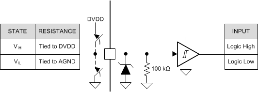
DRV8320 DRV8320R DRV8323 DRV8323R input_structure_01_slvsdj3.gifFigure 31. Logic-Level Input Pin Structure

Figure 32 shows the structure of the four level input pins, MODE and GAIN, on hardware interface devices. The input can be set with an external resistor.
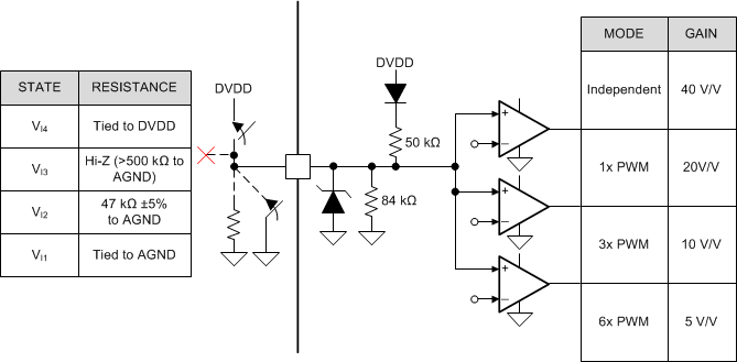
DRV8320 DRV8320R DRV8323 DRV8323R input_structure_02_slvsdj3.gifFigure 32. Four Level Input Pin Structure

Figure 33 shows the structure of the seven level input pins, IDRIVE and VDS, on hardware interface devices. The input can be set with an external resistor.
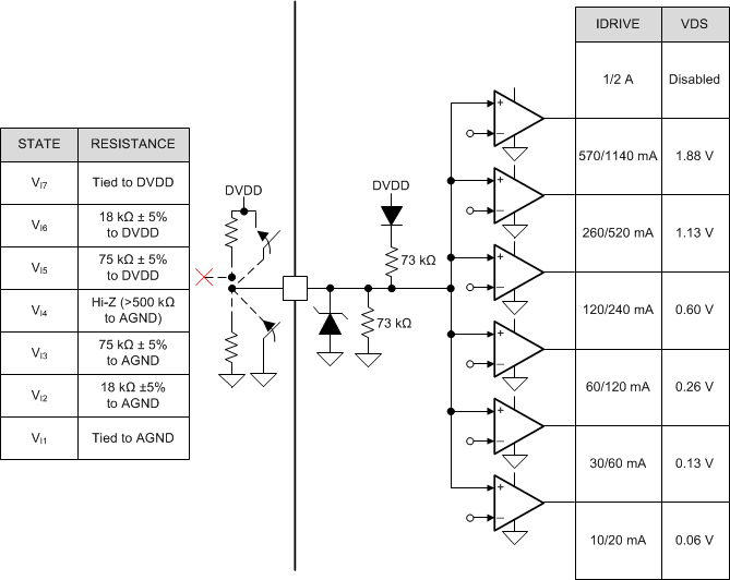
DRV8320 DRV8320R DRV8323 DRV8323R input_structure_03_slvsdj3.gifFigure 33. Seven Level Input Pin Structure

Figure 34 shows the structure of the open-drain output pins, nFAULT and SDO. The open-drain output requires an external pullup resistor to function correctly.
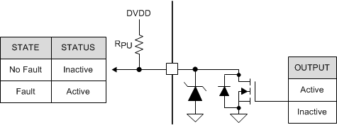
DRV8320 DRV8320R DRV8323 DRV8323R drv832xx_open_drain.gifFigure 34. Open-Drain Output Pin Structure