ZHCSP68C December 2021 – October 2022 DRV8328
PRODUCTION DATA
- 1 特性
- 2 应用
- 3 说明
- 4 Revision History
- 5 Device Comparison Table
- 6 Pin Configuration and Functions
- 7 Specification
-
8 Detailed Description
- 8.1 Overview
- 8.2 Functional Block Diagram
- 8.3
Feature Description
- 8.3.1 Three BLDC Gate Drivers
- 8.3.2 AVDD Linear Voltage Regulator
- 8.3.3 Pin Diagrams
- 8.3.4 Gate Driver Shutdown Sequence (DRVOFF)
- 8.3.5
Gate Driver Protective Circuits
- 8.3.5.1 PVDD Supply Undervoltage Lockout (PVDD_UV)
- 8.3.5.2 AVDD Power on Reset (AVDD_POR)
- 8.3.5.3 GVDD Undervoltage Lockout (GVDD_UV)
- 8.3.5.4 BST Undervoltage Lockout (BST_UV)
- 8.3.5.5 MOSFET VDS Overcurrent Protection (VDS_OCP)
- 8.3.5.6 VSENSE Overcurrent Protection (SEN_OCP)
- 8.3.5.7 Thermal Shutdown (OTSD)
- 8.4 Device Functional Modes
-
9 Application and Implementation
- 9.1 Application Information
- 9.2
Typical Application
- 9.2.1
Three Phase Brushless-DC Motor Control
- 9.2.1.1
Detailed Design Procedure
- 9.2.1.1.1 Motor Voltage
- 9.2.1.1.2 Bootstrap Capacitor and GVDD Capacitor Selection
- 9.2.1.1.3 Gate Drive Current
- 9.2.1.1.4 Gate Resistor Selection
- 9.2.1.1.5 System Considerations in High Power Designs
- 9.2.1.1.6 Dead Time Resistor Selection
- 9.2.1.1.7 VDSLVL Selection
- 9.2.1.1.8 AVDD Power Losses
- 9.2.1.1.9 Power Dissipation and Junction Temperature Losses
- 9.2.1.1
Detailed Design Procedure
- 9.2.2 Application Curves
- 9.2.1
Three Phase Brushless-DC Motor Control
- 10Power Supply Recommendations
- 11Layout
- 12Device and Documentation Support
- 13Mechanical, Packaging, and Orderable Information
8.3.2 AVDD Linear Voltage Regulator
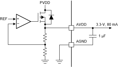
A 3.3-V, 80-mA linear regulator is available for use by external circuitry. The output of the LDO is fixed to 3.3-V. This regulator can provide the supply voltage for a low-power MCU or other circuitry with low supply current needs. The output of the AVDD regulator should be bypassed near the AVDD pin with a X5R or X7R, 1-µF, 6.3-V ceramic capacitor routed back to the AGND pin.
 Figure 8-5 AVDD Linear Regulator Block Diagram
The power dissipated in the device by the AVDD linear regulator can be calculated as follows: P = (VPVDD- VAVDD) x IAVDD
For example, at a VPVDD of 24 V, drawing 20 mA out of AVDD results in a power dissipation as shown in Equation 2.
Equation 2. 
