ZHCSQQ0A June 2022 – October 2022 DRV8329
PRODUCTION DATA
- 1 特性
- 2 应用
- 3 说明
- 4 Revision History
- 5 Device Comparison Table
- 6 Pin Configuration and Functions
- 7 Specification
-
8 Detailed Description
- 8.1 Overview
- 8.2 Functional Block Diagram
- 8.3
Feature Description
- 8.3.1 Three BLDC Gate Drivers
- 8.3.2 AVDD Linear Voltage Regulator
- 8.3.3 Pin Diagrams
- 8.3.4 Low-Side Current Sense Amplifiers
- 8.3.5 Gate Driver Shutdown Sequence (DRVOFF)
- 8.3.6
Gate Driver Protective Circuits
- 8.3.6.1 PVDD Supply Undervoltage Lockout (PVDD_UV)
- 8.3.6.2 AVDD Power on Reset (AVDD_POR)
- 8.3.6.3 GVDD Undervoltage Lockout (GVDD_UV)
- 8.3.6.4 BST Undervoltage Lockout (BST_UV)
- 8.3.6.5 MOSFET VDS Overcurrent Protection (VDS_OCP)
- 8.3.6.6 VSENSE Overcurrent Protection (SEN_OCP)
- 8.3.6.7 Thermal Shutdown (OTSD)
- 8.4 Device Functional Modes
-
9 Application and Implementation
- 9.1 Application Information
- 9.2
Typical Application
- 9.2.1
Three Phase Brushless-DC Motor Control
- 9.2.1.1
Detailed Design Procedure
- 9.2.1.1.1 Motor Voltage
- 9.2.1.1.2 Bootstrap Capacitor and GVDD Capacitor Selection
- 9.2.1.1.3 Gate Drive Current
- 9.2.1.1.4 Gate Resistor Selection
- 9.2.1.1.5 System Considerations in High Power Designs
- 9.2.1.1.6 Dead Time Resistor Selection
- 9.2.1.1.7 VDSLVL Selection
- 9.2.1.1.8 AVDD Power Losses
- 9.2.1.1.9 Current Sensing and Output Filtering
- 9.2.1.1.10 Power Dissipation and Junction Temperature Losses
- 9.2.1.1
Detailed Design Procedure
- 9.2.2 Application Curves
- 9.2.1
Three Phase Brushless-DC Motor Control
- 10Power Supply Recommendations
- 11Layout
- 12Device and Documentation Support
- 13Mechanical, Packaging, and Orderable Information
8.3.1.3.2 Deadtime and Cross-Conduction Prevention
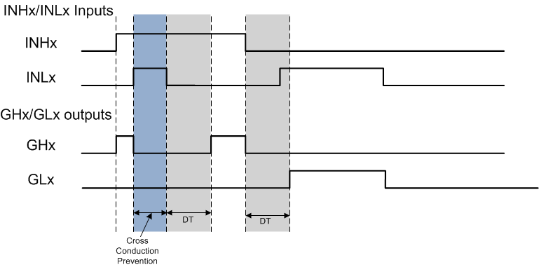
In the DRV8329, high- and low-side inputs operate independently, with an exception to prevent cross conduction when the high and low side of the same half-bridge are turned ON at same time. The device turns OFF high- and low- side output to prevent shoot through when high- and low-side inputs are logic high at same time.
The DRV8329 also provides dead time insertion to prevent both external MOSFETs of each half-bridge from switching on at the same time. In devices with a DT pin, deadtime can be linearly adjusted between 100 ns and 2000 ns by connecting s resistor between DT and ground. When the DT pin is left floating or connected to GND, a fixed deadtime of 55 ns (typical value) is inserted. The value of the resistor can be calculated using following equation.
 Figure 8-4 Cross Conduction Prevention and Deadtime Insertion