ZHCSQQ0A June 2022 – October 2022 DRV8329
PRODUCTION DATA
- 1 特性
- 2 应用
- 3 说明
- 4 Revision History
- 5 Device Comparison Table
- 6 Pin Configuration and Functions
- 7 Specification
-
8 Detailed Description
- 8.1 Overview
- 8.2 Functional Block Diagram
- 8.3
Feature Description
- 8.3.1 Three BLDC Gate Drivers
- 8.3.2 AVDD Linear Voltage Regulator
- 8.3.3 Pin Diagrams
- 8.3.4 Low-Side Current Sense Amplifiers
- 8.3.5 Gate Driver Shutdown Sequence (DRVOFF)
- 8.3.6
Gate Driver Protective Circuits
- 8.3.6.1 PVDD Supply Undervoltage Lockout (PVDD_UV)
- 8.3.6.2 AVDD Power on Reset (AVDD_POR)
- 8.3.6.3 GVDD Undervoltage Lockout (GVDD_UV)
- 8.3.6.4 BST Undervoltage Lockout (BST_UV)
- 8.3.6.5 MOSFET VDS Overcurrent Protection (VDS_OCP)
- 8.3.6.6 VSENSE Overcurrent Protection (SEN_OCP)
- 8.3.6.7 Thermal Shutdown (OTSD)
- 8.4 Device Functional Modes
-
9 Application and Implementation
- 9.1 Application Information
- 9.2
Typical Application
- 9.2.1
Three Phase Brushless-DC Motor Control
- 9.2.1.1
Detailed Design Procedure
- 9.2.1.1.1 Motor Voltage
- 9.2.1.1.2 Bootstrap Capacitor and GVDD Capacitor Selection
- 9.2.1.1.3 Gate Drive Current
- 9.2.1.1.4 Gate Resistor Selection
- 9.2.1.1.5 System Considerations in High Power Designs
- 9.2.1.1.6 Dead Time Resistor Selection
- 9.2.1.1.7 VDSLVL Selection
- 9.2.1.1.8 AVDD Power Losses
- 9.2.1.1.9 Current Sensing and Output Filtering
- 9.2.1.1.10 Power Dissipation and Junction Temperature Losses
- 9.2.1.1
Detailed Design Procedure
- 9.2.2 Application Curves
- 9.2.1
Three Phase Brushless-DC Motor Control
- 10Power Supply Recommendations
- 11Layout
- 12Device and Documentation Support
- 13Mechanical, Packaging, and Orderable Information
10.1 Bulk Capacitance Sizing
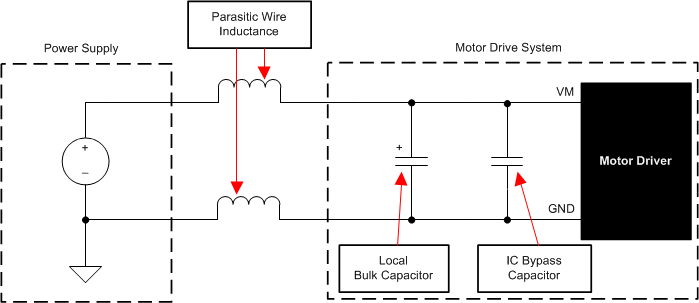
Having appropriate local bulk capacitance is an important factor in motor drive system design. It is generally beneficial to have more bulk capacitance, while the disadvantages are increased cost and physical size. The amount of local capacitance depends on a variety of factors including:
- The highest current required by the motor system
- The power supply's type, capacitance, and ability to source current
- The amount of parasitic inductance between the power supply and motor system
- The acceptable supply voltage ripple
- Type of motor (brushed DC, brushless DC, stepper)
- The motor startup and braking methods
The inductance between the power supply and motor drive system will limit the rate current can change from the power supply. If the local bulk capacitance is too small, the system will respond to excessive current demands or dumps from the motor with a change in voltage. When adequate bulk capacitance is used, the motor voltage remains stable and high current can be quickly supplied.
The data sheet provides a recommended minimum value, but system level testing is required to determine the appropriate sized bulk capacitor.
 Figure 10-1 Motor Drive Supply Parasitics Example