ZHCSIN3A August 2018 – June 2019 DRV8350 , DRV8350R , DRV8353 , DRV8353R
PRODUCTION DATA.
- 1 特性
- 2 应用
- 3 说明
- 4 修订历史记录
- 5 Device Comparison Table
- 6 Pin Configuration and Functions
- 7 Specifications
-
8 Detailed Description
- 8.1 Overview
- 8.2 Functional Block Diagram
- 8.3
Feature Description
- 8.3.1 Three Phase Smart Gate Drivers
- 8.3.2 DVDD Linear Voltage Regulator
- 8.3.3 Pin Diagrams
- 8.3.4 Low-Side Current-Shunt Amplifiers (DRV8353 and DRV8353R Only)
- 8.3.5 Step-Down Buck Regulator
- 8.3.6
Gate Driver Protective Circuits
- 8.3.6.1 VM Supply and VDRAIN Undervoltage Lockout (UVLO)
- 8.3.6.2 VCP Charge-Pump and VGLS Regulator Undervoltage Lockout (GDUV)
- 8.3.6.3 MOSFET VDS Overcurrent Protection (VDS_OCP)
- 8.3.6.4 VSENSE Overcurrent Protection (SEN_OCP)
- 8.3.6.5 Gate Driver Fault (GDF)
- 8.3.6.6 Overcurrent Soft Shutdown (OCP Soft)
- 8.3.6.7 Thermal Warning (OTW)
- 8.3.6.8 Thermal Shutdown (OTSD)
- 8.3.6.9 Fault Response Table
- 8.4 Device Functional Modes
- 8.5 Programming
- 8.6
Register Maps
- 8.6.1 Status Registers
- 8.6.2
Control Registers
- 8.6.2.1 Driver Control Register (address = 0x02h)
- 8.6.2.2 Gate Drive HS Register (address = 0x03h)
- 8.6.2.3 Gate Drive LS Register (address = 0x04h)
- 8.6.2.4 OCP Control Register (address = 0x05h)
- 8.6.2.5 CSA Control Register (DRV8353 and DRV8353R Only) (address = 0x06h)
- 8.6.2.6 Driver Configuration Register (DRV8353 and DRV8353R Only) (address = 0x07h)
-
9 Application and Implementation
- 9.1 Application Information
- 9.2
Typical Application
- 9.2.1
Primary Application
- 9.2.1.1 Design Requirements
- 9.2.1.2
Detailed Design Procedure
- 9.2.1.2.1 External MOSFET Support
- 9.2.1.2.2 IDRIVE Configuration
- 9.2.1.2.3 VDS Overcurrent Monitor Configuration
- 9.2.1.2.4 Sense-Amplifier Bidirectional Configuration (DRV8353 and DRV8353R)
- 9.2.1.2.5 Single Supply Power Dissipation
- 9.2.1.2.6 Single Supply Power Dissipation Example
- 9.2.1.2.7 Buck Regulator Configuration (DRV8350R and DRV8353R)
- 9.2.1.3 Application Curves
- 9.2.2 Alternative Application
- 9.2.1
Primary Application
- 10Power Supply Recommendations
- 11Layout
- 12器件和文档支持
- 13机械、封装和可订购信息
8.3.3 Pin Diagrams
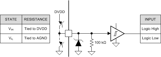
Figure 37 shows the input structure for the logic-level pins, INHx, INLx, ENABLE, nSCS, SCLK, and SDI.
 Figure 37. Logic-Level Input Pin Structure
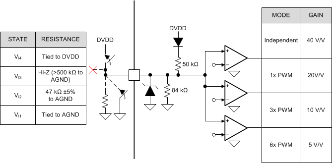
 Figure 38 shows the structure of the four level input pins, MODE and GAIN, on hardware interface devices. The input can be set with an external resistor.
 Figure 38. Four Level Input Pin Structure
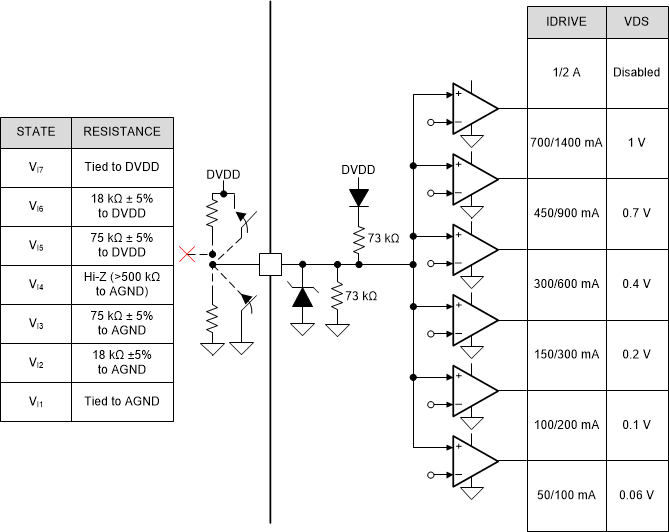
 Figure 39 shows the structure of the seven level input pins, IDRIVE and VDS, on hardware interface devices. The input can be set with an external resistor.
 Figure 39. Seven Level Input Pin Structure
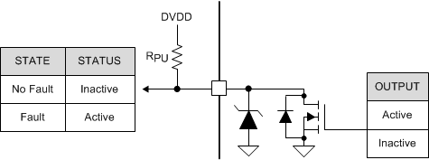
 Figure 40 shows the structure of the open-drain output pins nFAULT and SDO. The open-drain output requires an external pullup resistor to function correctly.
 Figure 40. Open-Drain Output Pin Structure