ZHCSIN3A August   2018  – June  2019 DRV8350 , DRV8350R , DRV8353 , DRV8353R

PRODUCTION DATA.  

  1. 特性
  2. 应用
  3. 说明
    1.     简化原理图
  4. 修订历史记录
  5. Device Comparison Table
  6. Pin Configuration and Functions
    1.     Pin Functions—32-Pin DRV8350 Devices
    2.     Pin Functions—48-Pin DRV8350R Devices
    3.     Pin Functions—40-Pin DRV8353 Devices
    4.     Pin Functions—48-Pin DRV8353R Devices
  7. Specifications
    1. 7.1 Absolute Maximum Ratings
    2. 7.2 ESD Ratings
    3. 7.3 Recommended Operating Conditions
    4. 7.4 Thermal Information
    5. 7.5 Electrical Characteristics
    6. 7.6 SPI Timing Requirements
    7. 7.7 Typical Characteristics
  8. Detailed Description
    1. 8.1 Overview
    2. 8.2 Functional Block Diagram
    3. 8.3 Feature Description
      1. 8.3.1 Three Phase Smart Gate Drivers
        1. 8.3.1.1 PWM Control Modes
          1. 8.3.1.1.1 6x PWM Mode (PWM_MODE = 00b or MODE Pin Tied to AGND)
          2. 8.3.1.1.2 3x PWM Mode (PWM_MODE = 01b or MODE Pin = 47 kΩ to AGND)
          3. 8.3.1.1.3 1x PWM Mode (PWM_MODE = 10b or MODE Pin = Hi-Z)
          4. 8.3.1.1.4 Independent PWM Mode (PWM_MODE = 11b or MODE Pin Tied to DVDD)
        2. 8.3.1.2 Device Interface Modes
          1. 8.3.1.2.1 Serial Peripheral Interface (SPI)
          2. 8.3.1.2.2 Hardware Interface
        3. 8.3.1.3 Gate Driver Voltage Supplies and Input Supply Configurations
        4. 8.3.1.4 Smart Gate Drive Architecture
          1. 8.3.1.4.1 IDRIVE: MOSFET Slew-Rate Control
          2. 8.3.1.4.2 TDRIVE: MOSFET Gate Drive Control
          3. 8.3.1.4.3 Propagation Delay
          4. 8.3.1.4.4 MOSFET VDS Monitors
          5. 8.3.1.4.5 VDRAIN Sense and Reference Pin
      2. 8.3.2 DVDD Linear Voltage Regulator
      3. 8.3.3 Pin Diagrams
      4. 8.3.4 Low-Side Current-Shunt Amplifiers (DRV8353 and DRV8353R Only)
        1. 8.3.4.1 Bidirectional Current Sense Operation
        2. 8.3.4.2 Unidirectional Current Sense Operation (SPI only)
        3. 8.3.4.3 Amplifier Calibration Modes
        4. 8.3.4.4 MOSFET VDS Sense Mode (SPI Only)
      5. 8.3.5 Step-Down Buck Regulator
        1. 8.3.5.1 Functional Block Diagram
        2. 8.3.5.2 Feature Description
          1. 8.3.5.2.1 Control Circuit Overview
          2. 8.3.5.2.2 Start-Up Regulator (VCC)
          3. 8.3.5.2.3 Regulation Comparator
          4. 8.3.5.2.4 Overvoltage Comparator
          5. 8.3.5.2.5 On-Time Generator and Shutdown
          6. 8.3.5.2.6 Current Limit
          7. 8.3.5.2.7 N-Channel Buck Switch and Driver
          8. 8.3.5.2.8 Thermal Protection
      6. 8.3.6 Gate Driver Protective Circuits
        1. 8.3.6.1 VM Supply and VDRAIN Undervoltage Lockout (UVLO)
        2. 8.3.6.2 VCP Charge-Pump and VGLS Regulator Undervoltage Lockout (GDUV)
        3. 8.3.6.3 MOSFET VDS Overcurrent Protection (VDS_OCP)
          1. 8.3.6.3.1 VDS Latched Shutdown (OCP_MODE = 00b)
          2. 8.3.6.3.2 VDS Automatic Retry (OCP_MODE = 01b)
          3. 8.3.6.3.3 VDS Report Only (OCP_MODE = 10b)
          4. 8.3.6.3.4 VDS Disabled (OCP_MODE = 11b)
        4. 8.3.6.4 VSENSE Overcurrent Protection (SEN_OCP)
          1. 8.3.6.4.1 VSENSE Latched Shutdown (OCP_MODE = 00b)
          2. 8.3.6.4.2 VSENSE Automatic Retry (OCP_MODE = 01b)
          3. 8.3.6.4.3 VSENSE Report Only (OCP_MODE = 10b)
          4. 8.3.6.4.4 VSENSE Disabled (OCP_MODE = 11b or DIS_SEN = 1b)
        5. 8.3.6.5 Gate Driver Fault (GDF)
        6. 8.3.6.6 Overcurrent Soft Shutdown (OCP Soft)
        7. 8.3.6.7 Thermal Warning (OTW)
        8. 8.3.6.8 Thermal Shutdown (OTSD)
        9. 8.3.6.9 Fault Response Table
    4. 8.4 Device Functional Modes
      1. 8.4.1 Gate Driver Functional Modes
        1. 8.4.1.1 Sleep Mode
        2. 8.4.1.2 Operating Mode
        3. 8.4.1.3 Fault Reset (CLR_FLT or ENABLE Reset Pulse)
      2. 8.4.2 Buck Regulator Functional Modes
        1. 8.4.2.1 Shutdown Mode
        2. 8.4.2.2 Active Mode
    5. 8.5 Programming
      1. 8.5.1 SPI Communication
        1. 8.5.1.1 SPI
          1. 8.5.1.1.1 SPI Format
    6. 8.6 Register Maps
      1. 8.6.1 Status Registers
        1. 8.6.1.1 Fault Status Register 1 (address = 0x00h)
          1. Table 11. Fault Status Register 1 Field Descriptions
        2. 8.6.1.2 Fault Status Register 2 (address = 0x01h)
          1. Table 12. Fault Status Register 2 Field Descriptions
      2. 8.6.2 Control Registers
        1. 8.6.2.1 Driver Control Register (address = 0x02h)
          1. Table 14. Driver Control Field Descriptions
        2. 8.6.2.2 Gate Drive HS Register (address = 0x03h)
          1. Table 15. Gate Drive HS Field Descriptions
        3. 8.6.2.3 Gate Drive LS Register (address = 0x04h)
          1. Table 16. Gate Drive LS Register Field Descriptions
        4. 8.6.2.4 OCP Control Register (address = 0x05h)
          1. Table 17. OCP Control Field Descriptions
        5. 8.6.2.5 CSA Control Register (DRV8353 and DRV8353R Only) (address = 0x06h)
          1. Table 18. CSA Control Field Descriptions
        6. 8.6.2.6 Driver Configuration Register (DRV8353 and DRV8353R Only) (address = 0x07h)
          1. Table 19. Driver Configuration Field Descriptions
  9. Application and Implementation
    1. 9.1 Application Information
    2. 9.2 Typical Application
      1. 9.2.1 Primary Application
        1. 9.2.1.1 Design Requirements
        2. 9.2.1.2 Detailed Design Procedure
          1. 9.2.1.2.1 External MOSFET Support
            1. 9.2.1.2.1.1 MOSFET Example
          2. 9.2.1.2.2 IDRIVE Configuration
            1. 9.2.1.2.2.1 IDRIVE Example
          3. 9.2.1.2.3 VDS Overcurrent Monitor Configuration
            1. 9.2.1.2.3.1 VDS Overcurrent Example
          4. 9.2.1.2.4 Sense-Amplifier Bidirectional Configuration (DRV8353 and DRV8353R)
            1. 9.2.1.2.4.1 Sense-Amplifier Example
          5. 9.2.1.2.5 Single Supply Power Dissipation
          6. 9.2.1.2.6 Single Supply Power Dissipation Example
          7. 9.2.1.2.7 Buck Regulator Configuration (DRV8350R and DRV8353R)
        3. 9.2.1.3 Application Curves
      2. 9.2.2 Alternative Application
        1. 9.2.2.1 Design Requirements
        2. 9.2.2.2 Detailed Design Procedure
          1. 9.2.2.2.1 Sense Amplifier Unidirectional Configuration
            1. 9.2.2.2.1.1 Sense-Amplifier Example
            2. 9.2.2.2.1.2 Dual Supply Power Dissipation
            3. 9.2.2.2.1.3 Dual Supply Power Dissipation Example
  10. 10Power Supply Recommendations
    1. 10.1 Bulk Capacitance Sizing
  11. 11Layout
    1. 11.1 Layout Guidelines
      1. 11.1.1 Buck-Regulator Layout Guidelines
    2. 11.2 Layout Example
  12. 12器件和文档支持
    1. 12.1 器件支持
      1. 12.1.1 器件命名规则
    2. 12.2 文档支持
      1. 12.2.1 相关文档
    3. 12.3 相关链接
    4. 12.4 接收文档更新通知
    5. 12.5 社区资源
    6. 12.6 商标
    7. 12.7 静电放电警告
    8. 12.8 Glossary
  13. 13机械、封装和可订购信息

封装选项

机械数据 (封装 | 引脚)
散热焊盘机械数据 (封装 | 引脚)
订购信息

Alternative Application

In this application, the DRV8353R is configured to use one sense amplifier in unidirectional mode for a summing current sense scheme often used in trapezoidal or hall-based BLDC commutation control. Additionally, the device is configured in dual supply mode using the integrated buck regulator for the VM gate drive voltage supply to decrease internal power dissipation.
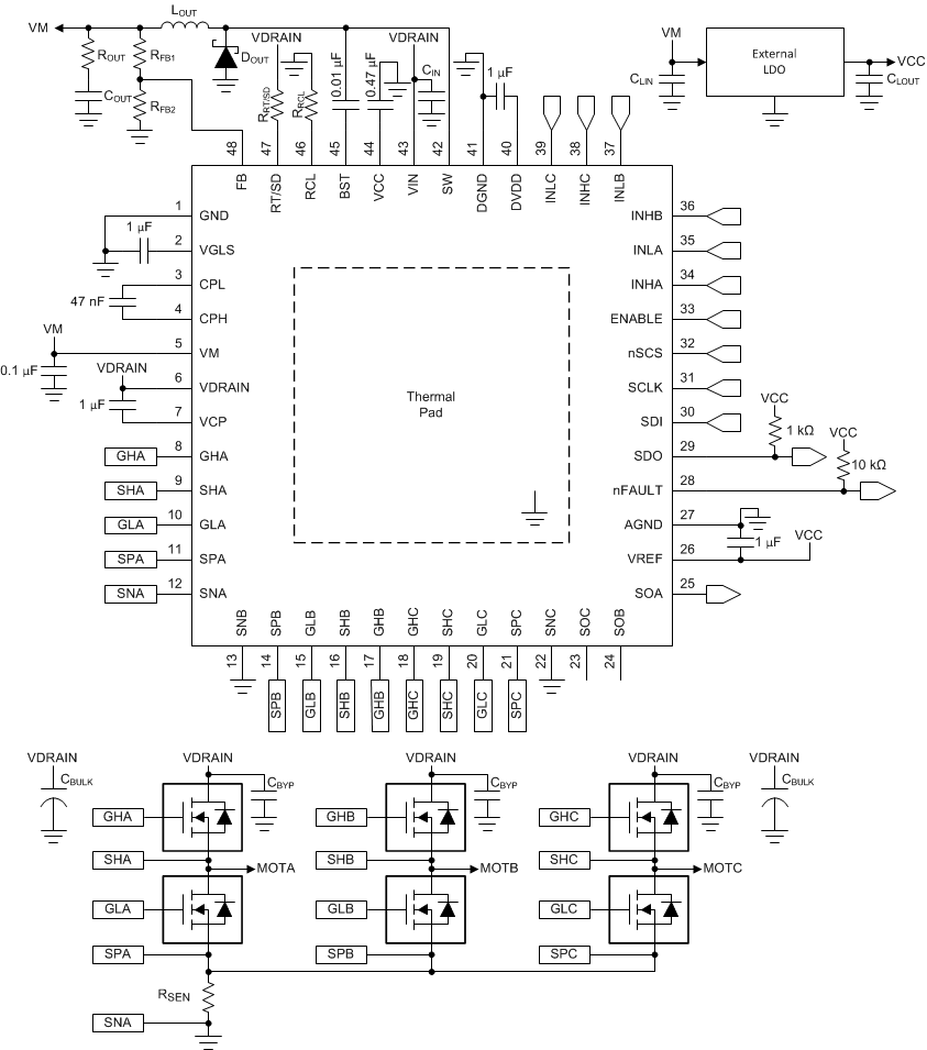
DRV8350 DRV8350R DRV8353 DRV8353R drv835x-secondary-app.gifFigure 73. Alternative Application Schematic