ZHCSIN3A August 2018 – June 2019 DRV8350 , DRV8350R , DRV8353 , DRV8353R
PRODUCTION DATA.
- 1 特性
- 2 应用
- 3 说明
- 4 修订历史记录
- 5 Device Comparison Table
- 6 Pin Configuration and Functions
- 7 Specifications
-
8 Detailed Description
- 8.1 Overview
- 8.2 Functional Block Diagram
- 8.3
Feature Description
- 8.3.1 Three Phase Smart Gate Drivers
- 8.3.2 DVDD Linear Voltage Regulator
- 8.3.3 Pin Diagrams
- 8.3.4 Low-Side Current-Shunt Amplifiers (DRV8353 and DRV8353R Only)
- 8.3.5 Step-Down Buck Regulator
- 8.3.6
Gate Driver Protective Circuits
- 8.3.6.1 VM Supply and VDRAIN Undervoltage Lockout (UVLO)
- 8.3.6.2 VCP Charge-Pump and VGLS Regulator Undervoltage Lockout (GDUV)
- 8.3.6.3 MOSFET VDS Overcurrent Protection (VDS_OCP)
- 8.3.6.4 VSENSE Overcurrent Protection (SEN_OCP)
- 8.3.6.5 Gate Driver Fault (GDF)
- 8.3.6.6 Overcurrent Soft Shutdown (OCP Soft)
- 8.3.6.7 Thermal Warning (OTW)
- 8.3.6.8 Thermal Shutdown (OTSD)
- 8.3.6.9 Fault Response Table
- 8.4 Device Functional Modes
- 8.5 Programming
- 8.6
Register Maps
- 8.6.1 Status Registers
- 8.6.2
Control Registers
- 8.6.2.1 Driver Control Register (address = 0x02h)
- 8.6.2.2 Gate Drive HS Register (address = 0x03h)
- 8.6.2.3 Gate Drive LS Register (address = 0x04h)
- 8.6.2.4 OCP Control Register (address = 0x05h)
- 8.6.2.5 CSA Control Register (DRV8353 and DRV8353R Only) (address = 0x06h)
- 8.6.2.6 Driver Configuration Register (DRV8353 and DRV8353R Only) (address = 0x07h)
-
9 Application and Implementation
- 9.1 Application Information
- 9.2
Typical Application
- 9.2.1
Primary Application
- 9.2.1.1 Design Requirements
- 9.2.1.2
Detailed Design Procedure
- 9.2.1.2.1 External MOSFET Support
- 9.2.1.2.2 IDRIVE Configuration
- 9.2.1.2.3 VDS Overcurrent Monitor Configuration
- 9.2.1.2.4 Sense-Amplifier Bidirectional Configuration (DRV8353 and DRV8353R)
- 9.2.1.2.5 Single Supply Power Dissipation
- 9.2.1.2.6 Single Supply Power Dissipation Example
- 9.2.1.2.7 Buck Regulator Configuration (DRV8350R and DRV8353R)
- 9.2.1.3 Application Curves
- 9.2.2 Alternative Application
- 9.2.1
Primary Application
- 10Power Supply Recommendations
- 11Layout
- 12器件和文档支持
- 13机械、封装和可订购信息
8.3.1.4.4 MOSFET VDS Monitors
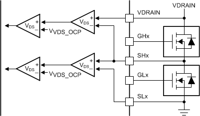
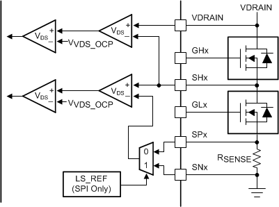
The gate drivers implement adjustable VDS voltage monitors to detect overcurrent or short-circuit conditions on the external power MOSFETs. When the monitored voltage is greater than the VDS trip point (VVDS_OCP) for longer than the deglitch time (tOCP), an overcurrent condition is detected and action is taken according to the device VDS fault mode.
The high-side VDS monitors measure the voltage between the VDRAIN and SHx pins. In devices with three current-shunt amplifiers (DRV8353 and DRV8353R), the low-side VDS monitors measure the voltage between the SHx and SPx pins. If the current shunt amplifier is unused, tie the SP pins to the common ground point of the external half-bridges. On device options without the current shunt amplifiers (DRV8350 and DRV8350R) the low-side VDS monitor measures between the SHx and SLx pins.
For the SPI devices, the low-side VDS monitor reference point can be changed between the SPx and SNx pins if desired with the LS_REF register setting. This is only for the low-side VDS monitor. The high-side VDS monitor stays between the VDRAIN and SHx pins.
The VVDS_OCP threshold is programmable between 0.06 V and 2 V on SPI device and between 0.06 V and 1 V on hardware interface devices. Additional information on the VDS monitor levels are described in the Register Maps section for SPI devices and in the Pin Diagrams section hardware interface device.
 Figure 34. DRV8350 and DRV8350R VDS Monitors
  Figure 35. DRV8353 and DRV8353R VDS Monitors