ZHCSIN3A August 2018 – June 2019 DRV8350 , DRV8350R , DRV8353 , DRV8353R
PRODUCTION DATA.
- 1 特性
- 2 应用
- 3 说明
- 4 修订历史记录
- 5 Device Comparison Table
- 6 Pin Configuration and Functions
- 7 Specifications
-
8 Detailed Description
- 8.1 Overview
- 8.2 Functional Block Diagram
- 8.3
Feature Description
- 8.3.1 Three Phase Smart Gate Drivers
- 8.3.2 DVDD Linear Voltage Regulator
- 8.3.3 Pin Diagrams
- 8.3.4 Low-Side Current-Shunt Amplifiers (DRV8353 and DRV8353R Only)
- 8.3.5 Step-Down Buck Regulator
- 8.3.6
Gate Driver Protective Circuits
- 8.3.6.1 VM Supply and VDRAIN Undervoltage Lockout (UVLO)
- 8.3.6.2 VCP Charge-Pump and VGLS Regulator Undervoltage Lockout (GDUV)
- 8.3.6.3 MOSFET VDS Overcurrent Protection (VDS_OCP)
- 8.3.6.4 VSENSE Overcurrent Protection (SEN_OCP)
- 8.3.6.5 Gate Driver Fault (GDF)
- 8.3.6.6 Overcurrent Soft Shutdown (OCP Soft)
- 8.3.6.7 Thermal Warning (OTW)
- 8.3.6.8 Thermal Shutdown (OTSD)
- 8.3.6.9 Fault Response Table
- 8.4 Device Functional Modes
- 8.5 Programming
- 8.6
Register Maps
- 8.6.1 Status Registers
- 8.6.2
Control Registers
- 8.6.2.1 Driver Control Register (address = 0x02h)
- 8.6.2.2 Gate Drive HS Register (address = 0x03h)
- 8.6.2.3 Gate Drive LS Register (address = 0x04h)
- 8.6.2.4 OCP Control Register (address = 0x05h)
- 8.6.2.5 CSA Control Register (DRV8353 and DRV8353R Only) (address = 0x06h)
- 8.6.2.6 Driver Configuration Register (DRV8353 and DRV8353R Only) (address = 0x07h)
-
9 Application and Implementation
- 9.1 Application Information
- 9.2
Typical Application
- 9.2.1
Primary Application
- 9.2.1.1 Design Requirements
- 9.2.1.2
Detailed Design Procedure
- 9.2.1.2.1 External MOSFET Support
- 9.2.1.2.2 IDRIVE Configuration
- 9.2.1.2.3 VDS Overcurrent Monitor Configuration
- 9.2.1.2.4 Sense-Amplifier Bidirectional Configuration (DRV8353 and DRV8353R)
- 9.2.1.2.5 Single Supply Power Dissipation
- 9.2.1.2.6 Single Supply Power Dissipation Example
- 9.2.1.2.7 Buck Regulator Configuration (DRV8350R and DRV8353R)
- 9.2.1.3 Application Curves
- 9.2.2 Alternative Application
- 9.2.1
Primary Application
- 10Power Supply Recommendations
- 11Layout
- 12器件和文档支持
- 13机械、封装和可订购信息
8.3.4.4 MOSFET VDS Sense Mode (SPI Only)
The current-sense amplifiers on the DRV8353 and DRV8353R SPI devices can be configured to amplify the voltage across the external low-side MOSFET VDS. This allows for the external controller to measure the voltage drop across the MOSFET RDS(on) without the shunt resistor and then calculate the half-bridge current level.
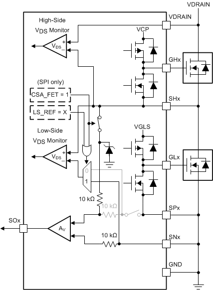
To enable this mode set the CSA_FET bit to 1. The positive input of the amplifier is then internally connected to the SHx pin with an internal clamp to prevent high voltage on the SHx pin from damaging the sense amplifier inputs. During this mode of operation, the SPx pins should stay connected to the source of the low-side MOSFET as it serves as the reference for the low-side gate driver. When the CSA_FET bit is set to 1, the negative reference for the low-side VDS monitor is automatically set to SNx, regardless of the state of the LS_REF bit state. This setting is implemented to prevent disabling of the low-side VDS monitor.
If the system operates in MOSFET VDS sensing mode, route the SHx and SNx pins with Kelvin connections across the drain and source of the external low-side MOSFETs.
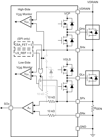
 Figure 48. Resistor Sense Configuration
  Figure 49. VDS Sense Configuration
 When operating in MOSFET VDS sense mode, the amplifier is enabled at the end of the tDRIVE time. At this time, the amplifier input is connected to the SHx pin, and the SOx output is valid. When the low-side MOSFET receives a signal to turn off, the amplifier inputs, SPx and SNx, are shorted together internally.