ZHCSIN3A August 2018 – June 2019 DRV8350 , DRV8350R , DRV8353 , DRV8353R
PRODUCTION DATA.
- 1 特性
- 2 应用
- 3 说明
- 4 修订历史记录
- 5 Device Comparison Table
- 6 Pin Configuration and Functions
- 7 Specifications
-
8 Detailed Description
- 8.1 Overview
- 8.2 Functional Block Diagram
- 8.3
Feature Description
- 8.3.1 Three Phase Smart Gate Drivers
- 8.3.2 DVDD Linear Voltage Regulator
- 8.3.3 Pin Diagrams
- 8.3.4 Low-Side Current-Shunt Amplifiers (DRV8353 and DRV8353R Only)
- 8.3.5 Step-Down Buck Regulator
- 8.3.6
Gate Driver Protective Circuits
- 8.3.6.1 VM Supply and VDRAIN Undervoltage Lockout (UVLO)
- 8.3.6.2 VCP Charge-Pump and VGLS Regulator Undervoltage Lockout (GDUV)
- 8.3.6.3 MOSFET VDS Overcurrent Protection (VDS_OCP)
- 8.3.6.4 VSENSE Overcurrent Protection (SEN_OCP)
- 8.3.6.5 Gate Driver Fault (GDF)
- 8.3.6.6 Overcurrent Soft Shutdown (OCP Soft)
- 8.3.6.7 Thermal Warning (OTW)
- 8.3.6.8 Thermal Shutdown (OTSD)
- 8.3.6.9 Fault Response Table
- 8.4 Device Functional Modes
- 8.5 Programming
- 8.6
Register Maps
- 8.6.1 Status Registers
- 8.6.2
Control Registers
- 8.6.2.1 Driver Control Register (address = 0x02h)
- 8.6.2.2 Gate Drive HS Register (address = 0x03h)
- 8.6.2.3 Gate Drive LS Register (address = 0x04h)
- 8.6.2.4 OCP Control Register (address = 0x05h)
- 8.6.2.5 CSA Control Register (DRV8353 and DRV8353R Only) (address = 0x06h)
- 8.6.2.6 Driver Configuration Register (DRV8353 and DRV8353R Only) (address = 0x07h)
-
9 Application and Implementation
- 9.1 Application Information
- 9.2
Typical Application
- 9.2.1
Primary Application
- 9.2.1.1 Design Requirements
- 9.2.1.2
Detailed Design Procedure
- 9.2.1.2.1 External MOSFET Support
- 9.2.1.2.2 IDRIVE Configuration
- 9.2.1.2.3 VDS Overcurrent Monitor Configuration
- 9.2.1.2.4 Sense-Amplifier Bidirectional Configuration (DRV8353 and DRV8353R)
- 9.2.1.2.5 Single Supply Power Dissipation
- 9.2.1.2.6 Single Supply Power Dissipation Example
- 9.2.1.2.7 Buck Regulator Configuration (DRV8350R and DRV8353R)
- 9.2.1.3 Application Curves
- 9.2.2 Alternative Application
- 9.2.1
Primary Application
- 10Power Supply Recommendations
- 11Layout
- 12器件和文档支持
- 13机械、封装和可订购信息
8.3.5.2.2 Start-Up Regulator (VCC)
The high voltage bias regulator is integrated within the LM5008A. The input pin (VIN) can be connected directly to line voltages between 6 V and 95 V, with transient capability to 100 V. Referring to the Figure 50, when VIN is between 6 V and the bypass threshold (nominally 8.5 V), the bypass switch (Q2) is on, and VCC tracks VIN within 100 mV to 150 mV. The bypass switch on-resistance is approximately 100 Ω, with inherent current limiting at approximately 100 mA. When VIN is above the bypass threshold Q2 is turned off, and VCC is regulated at 7 V. The VCC regulator output current is limited at approximately 9.2 mA. When the LM5008A is shut down using the RT/SD pin, the VCC bypass switch is shut off regardless of the voltage at VIN.
When VIN exceeds the bypass threshold, the time required for Q2 to shut off is approximately 2 µs to 3 µs. The capacitor at VCC (C3) must be a minimum of 0.47 µF to prevent the voltage at VCC from rising above its absolute maximum rating in response to a step input applied at VIN. C3 must be placed as near as possible to the VCC and RTN pins. In applications with a relatively high input voltage, power dissipation in the bias regulator is a concern. An auxiliary voltage of between 7.5 V and 14 V can be diode connected to the VCC pin to shut off the VCC regulator, thereby reducing internal power dissipation. The current required into the VCC pin is shown in the typical characteristics curves. Internally a diode connects VCC to VIN requiring that the auxiliary voltage be less than VIN.
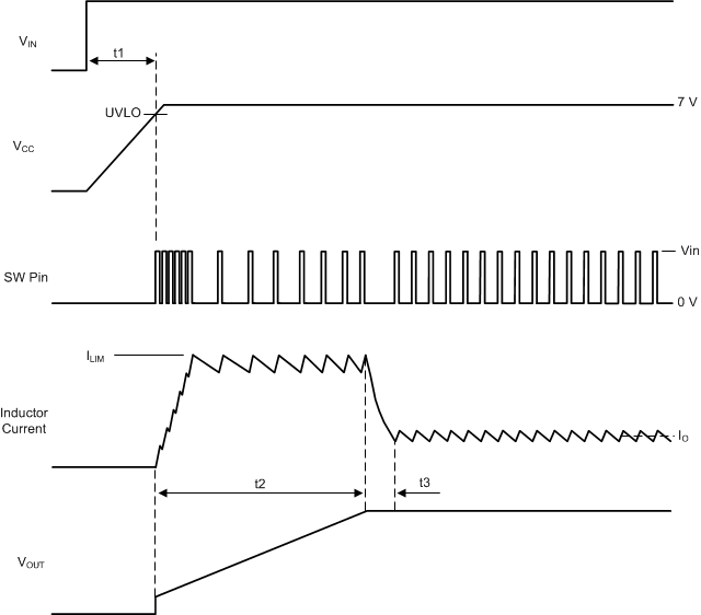
The turnon sequence is shown in Figure 52. During the initial delay (t1), VCC ramps up at a rate determined by its current limit and C3 while internal circuitry stabilizes. When VCC reaches the upper threshold of its undervoltage lockout (UVLO, typically 5.3 V), the buck switch is enabled. The inductor current increases to the current limit threshold (ILIM), and during t2 the VOUT increases as the output capacitor charges up. When VOUT reaches the intended voltage the average inductor current decreases (t3) to the nominal load current (IO).
 Figure 52. Start-Up Sequence