ZHCSR67 July 2020 DRV8353M
PRODUCTION DATA
- 1 特性
- 2 应用
- 3 说明
- 4 Revision History
- 5 Device Comparison Table
- 6 Pin Configuration and Functions
- 7 Absolute Maximum Ratings
- 8 ESD Ratings
- 9 Recommended Operating Conditions
- 10Thermal Information
- 11Electrical Characteristics
- 12SPI Timing Requirements
-
13Detailed Description
- 13.1 Overview
- 13.2 Functional Block Diagram
- 13.3
Feature Description
- 13.3.1 Three Phase Smart Gate Drivers
- 13.3.2 DVDD Linear Voltage Regulator
- 13.3.3 Pin Diagrams
- 13.3.4 Low-Side Current-Shunt Amplifiers
- 13.3.5
Gate Driver Protective Circuits
- 13.3.5.1 VM Supply and VDRAIN Undervoltage Lockout (UVLO)
- 13.3.5.2 VCP Charge-Pump and VGLS Regulator Undervoltage Lockout (GDUV)
- 13.3.5.3 MOSFET VDS Overcurrent Protection (VDS_OCP)
- 13.3.5.4 VSENSE Overcurrent Protection (SEN_OCP)
- 13.3.5.5 Gate Driver Fault (GDF)
- 13.3.5.6 Overcurrent Soft Shutdown (OCP Soft)
- 13.3.5.7 Thermal Warning (OTW)
- 13.3.5.8 Thermal Shutdown (OTSD)
- 13.3.5.9 Fault Response Table
- 13.4 Device Functional Modes
- 13.5 Programming
- 13.6
Register Maps
- 13.6.1 Status Registers
- 13.6.2
Control Registers
- 13.6.2.1 Driver Control Register (address = 0x02h)
- 13.6.2.2 Gate Drive HS Register (address = 0x03h)
- 13.6.2.3 Gate Drive LS Register (address = 0x04h)
- 13.6.2.4 OCP Control Register (address = 0x05h)
- 13.6.2.5 CSA Control Register (address = 0x06h)
- 13.6.2.6 Driver Configuration Register (address = 0x07h)
-
14Application and Implementation
- 14.1 Application Information
- 14.2
Typical Application
- 14.2.1
Primary Application
- 14.2.1.1 Design Requirements
- 14.2.1.2 Detailed Design Procedure
- 14.2.1.3 Application Curves
- 14.2.1
Primary Application
- 15Power Supply Recommendations
- 16Layout
- 17Device and Documentation Support
- 18Mechanical, Packaging, and Orderable Information
13.3.4.3 Amplifier Calibration Modes
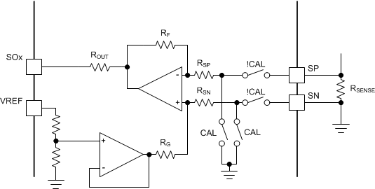
To minimize DC offset and drift over temperature, a DC calibration mode is provided and enabled through the SPI register (CSA_CAL_X). This option is not available on hardware interface devices. When the calibration setting is enabled the inputs to the amplifier are shorted and the load is disconnected. DC calibration can be done at any time, even when the half-bridges are operating. For the best results, do the DC calibration during the switching OFF period to decrease the potential noise impact to the amplifier. A diagram of the calibration mode is shown below. When a CSA_CAL_X bit is enabled, the corresponding amplifier goes to the calibration mode.
 Figure 13-27 Amplifier Manual Calibration
In addition to the manual calibration method provided on the SPI devices versions, the DRV8353M family of devices provide an auto calibration feature on both the hardware and SPI device versions in order to minimize the amplifier input offset after power up and during run time to account for temperature and device variation.
Auto calibration occurs automatically on device power up for both the hardware and SPI device options. The power up auto calibration starts immediately after the VREF pin crosses the minimum operational VREF voltage. 50 us should be allowed for the power up auto calibration routine to complete after the VREF pin voltage crosses the minimum VREF operational voltage. The auto calibration functions by doing a trim routine of the amplifier to minimize the amplifier input offset. After this the amplifiers are ready for normal operation.
For the SPI device options, auto calibration can also be done again during run time by enabling the AUTO_CAL register setting. Auto calibration can then be commanded with the corresponding CSA_CAL_X register setting to rerun the auto calibration routine. During auto calibration all of the amplifiers will be configured for the max gain setting in order to improve the accuracy of the calibration routine.