ZHCS389C June   2011  – December 2022 DRV8662

PRODUCTION DATA  

  1. 特性
  2. 应用
  3. 说明
  4. Revision History
  5. Pin Configuration and Functions
  6. Specifications
    1. 6.1 Absolute Maximum Ratings
    2. 6.2 ESD Ratings
    3. 6.3 Recommended Operating Conditions
    4. 6.4 Thermal Information
    5. 6.5 Electrical Characteristics
    6. 6.6 Timing Requirements
    7. 6.7 Typical Characteristics
  7. Detailed Description
    1. 7.1 Overview
    2. 7.2 Functional Block Diagram
    3. 7.3 Feature Description
      1. 7.3.1 Fast Start-up (Enable Pin)
      2. 7.3.2 Gain Control
      3. 7.3.3 Adjustable Boost Voltage
      4. 7.3.4 Adjustable Boost Current Limit
      5. 7.3.5 Internal Charge Pump
      6. 7.3.6 Thermal Shutdown
    4. 7.4 Device Functional Modes
      1. 7.4.1 Startup/shutdown Sequencing
        1. 7.4.1.1 PWM Source
        2. 7.4.1.2 DAC Source
      2. 7.4.2 Low-voltage Operation
    5. 7.5 Programming
      1. 7.5.1 Programming the Boost Voltage
      2. 7.5.2 Programing the Boost Current Limit
  8. Application and Implementation
    1. 8.1 Application Information
    2. 8.2 Typical Application
      1. 8.2.1 DRV8662 System Diagram with DAC Input
        1. 8.2.1.1 Design Requirements
        2. 8.2.1.2 Detailed Design Procedure
          1. 8.2.1.2.1 Inductor Selection
          2. 8.2.1.2.2 Piezo Actuator Selection
          3. 8.2.1.2.3 Boost Capacitor Selection
          4. 8.2.1.2.4 Current Consumption Calculation
          5. 8.2.1.2.5 Input Filter Considerations
        3. 8.2.1.3 Application Curves
      2. 8.2.2 DRV8662 System Diagram with Filtered Single-Ended PWM Input
        1. 8.2.2.1 Design Requirements
        2. 8.2.2.2 Detailed Design Procedure
          1. 8.2.2.2.1 Input Filter Design
        3. 8.2.2.3 Application Curves
  9. Power Supply Recommendations
  10. 10Layout
    1. 10.1 Layout Guidelines
    2. 10.2 Layout Example
  11. 11Device and Documentation Support
    1. 11.1 Documentation Support
      1. 11.1.1 Related Documentation
    2. 11.2 Trademarks
  12. 12Mechanical, Packaging, and Orderable Information

封装选项

机械数据 (封装 | 引脚)
散热焊盘机械数据 (封装 | 引脚)
订购信息

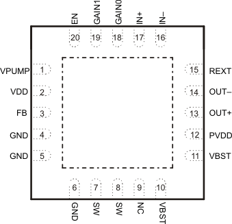
Pin Configuration and Functions

GUID-3F0FD50A-783F-4849-80D8-AD912F2AE2A9-low.gifFigure 5-1 QFN (RGP)Top View
Table 5-1 Pin Functions
PIN INPUT/ OUTPUT/ POWER (I/O/P) DESCRIPTION
NAME NO. (RGP)
EN 20 I Chip enable
FB 3 I Boost feedback
GAIN0 18 I Gain programming pin – LSB
GAIN1 19 I Gain programming pin – MSB
GND 4, 5, 6 P Ground
IN+ 17 I Non-inverting input (If unused, connect to GND through capacitor)
IN– 16 I Inverting input (If unused, connect to GND through capacitor)
OUT+ 13 O Non-inverting output
OUT– 14 O Inverting output
PVDD 12 P Amplifier supply voltage
REXT 15 I Resistor to ground, sets boost current limit
SW 7, 8 P Internal boost switch pin
VBST 10, 11 P Boost output voltage
VDD 2 P Power supply (connect to battery)
VPUMP 1 P Internal Charge-pump voltage