ZHCSDO0A March 2015 – May 2015 DRV8701
PRODUCTION DATA.
- 1 特性
- 2 应用
- 3 说明
- 4 修订历史记录
- 5 Pin Configuration and Functions
- 6 Specifications
-
7 Detailed Description
- 7.1 Overview
- 7.2 Functional Block Diagram
- 7.3
Feature Description
- 7.3.1 Bridge Control
- 7.3.2 Half-Bridge Operation
- 7.3.3 Current Regulation
- 7.3.4 Amplifier Output SO
- 7.3.5 PWM Motor Gate Drivers
- 7.3.6 IDRIVE Pin
- 7.3.7 Dead Time
- 7.3.8 Propagation Delay
- 7.3.9 Overcurrent VDS Monitor
- 7.3.10 Charge Pump
- 7.3.11 LDO Voltage Regulators
- 7.3.12 Gate Drive Clamp
- 7.3.13 Protection Circuits
- 7.3.14 Reverse Supply Protection
- 7.4 Device Functional Modes
- 8 Application and Implementation
- 9 Power Supply Recommendations
- 10Layout
- 11器件和文档支持
- 12机械、封装和可订购信息
5 Pin Configuration and Functions
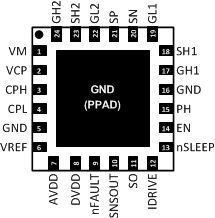
RGE Package
|
RGE Package
|
DRV8701E (PH/EN)
| PIN | TYPE | DESCRIPTION | ||
|---|---|---|---|---|
| NAME | NO. | |||
| EN | 14 | Input | Bridge enable input | Logic low places the bridge in brake mode; see Table 1 |
| PH | 15 | Input | Bridge phase input | Controls the direction of the H-bridge; see Table 1 |
DRV8701P (PWM)
| PIN | TYPE | DESCRIPTION | ||
|---|---|---|---|---|
| NAME | NO. | |||
| IN1 | 15 | Input | Bridge PWM input | Logic controls the state of H-bridge; see Table 2 |
| IN2 | 14 | Input | ||
Common Pins
| PIN | TYPE | DESCRIPTION | ||
|---|---|---|---|---|
| NAME | NO. | |||
| VM | 1 | Power | Power supply | Connect to motor supply voltage; bypass to GND with a 0.1-µF ceramic plus a 10-µF minimum capacitor rated for VM; additional capacitance may be required based on drive current |
| GND | 5 | Power | Device ground | Must be connected to ground |
| 16 | ||||
| PPAD | ||||
| VCP | 2 | Power | Charge pump output | Connect a 16-V, 1-µF ceramic capacitor to VM |
| CPH | 3 | Power | Charge pump switching nodes | Connect a 0.1-µF X7R capacitor rated for VM between CPH and CPL |
| CPL | 4 | |||
| DVDD | 8 | Power | Logic regulator | 3.3-V logic supply regulator; bypass to GND with a 6.3-V, 1-µF ceramic capacitor |
| AVDD | 7 | Power | Analog regulator | 4.8-V analog supply regulator; bypass to GND with a 6.3-V, 1-µF ceramic capacitor |
| nSLEEP | 13 | Input | Device sleep mode | Pull logic low to put device into a low-power sleep mode with FETs High-Z; internal pulldown |
| IDRIVE | 12 | Input | Gate drive current setting pin | Resistor value or voltage forced on this pin sets the gate drive current; see applications section for more details |
| VREF | 6 | Input | Analog reference input | Controls the current regulation; apply a voltage between 0.3 V and AVDD |
| nFAULT | 9 | Open Drain | Fault indication pin | Pulled logic low with fault condition; open-drain output requires an external pullup |
| SNSOUT | 10 | Open Drain | Sense comparator output | Pulled logic low when the drive current hits the current chopping threshold; open-drain output requires an external pullup |
| SO | 11 | Output | Shunt amplifier output | Voltage on this pin is equal to the SP voltage times AV plus an offset; place no more than 1 nF of capacitance on this pin |
| SN | 20 | Input | Shunt amplifier negative input | Connect to SP through current sense resistor and to GND |
| SP | 21 | Input | Shunt amplifier positive input | Connect to low-side FET source and to SN through current sense resistor |
| GH1 | 17 | Output | High-side gate | Connect to high-side FET gate |
| GH2 | 24 | |||
| GL1 | 19 | Output | Low-side gate | Connect to low-side FET gate |
| GL2 | 22 | |||
| SH1 | 18 | Input | Phase node | Connect to high-side FET source and low-side FET drain |
| SH2 | 23 | |||
External Passive Components
| COMPONENT | PIN 1 | PIN 2 | RECOMMENDED |
|---|---|---|---|
| CVM1 | VM | GND | 0.1-µF ceramic capacitor rated for VM |
| CVM2 | VM | GND | ≥10-µF capacitor rated for VM |
| CVCP | VCP | VM | 16-V, 1-µF ceramic capacitor |
| CSW | CPH | CPL | 0.1-µF X7R capacitor rated for VM |
| CDVDD | DVDD | GND | 6.3-V, 1-µF ceramic capacitor |
| CAVDD | AVDD | GND | 6.3-V, 1-µF ceramic capacitor |
| RIDRIVE | IDRIVE | GND | See Typical Applicationsfor resistor sizing |
| RnFAULT | VCC(1) | nFAULT | ≥10-kΩ pullup |
| RSNSOUT | VCC(1) | SNSOUT | ≥10-kΩ pullup |
| RSENSE | SP | SN/GND | Optional low-side sense resistor |
(1) VCC is not a pin on the DRV8701, but a VCC supply voltage pullup is required for open-drain outputs nFAULT and SNSOUT. The system controller supply can be used for this pullup voltage, or these pins can be pulled up to either AVDD or DVDD.
External FETs
| Component | Gate | Drain | Source | Recommended |
|---|---|---|---|---|
| QHS1 | GH1 | VM | SH1 | Supports up to 200-nC FETs at 40-kHz PWM; see Detailed Design Procedure for more details |
| QLS1 | GL1 | SH1 | SP or GND | |
| QHS2 | GH2 | VM | SH2 | |
| QLS2 | GL2 | SH2 | SP or GND |

