ZHCSG08E October 2016 – January 2021 DRV8702-Q1 , DRV8703-Q1
PRODUCTION DATA
- 1 特性
- 2 应用
- 3 说明
- 4 Revision History
- 5 Pin Configuration and Functions
- 6 Specifications
-
7 Detailed Description
- 7.1 Overview
- 7.2 Functional Block Diagram
- 7.3
Feature Description
- 7.3.1 Bridge Control
- 7.3.2 MODE Pin
- 7.3.3 nFAULT Pin
- 7.3.4 Current Regulation
- 7.3.5 Amplifier Output (SO)
- 7.3.6 PWM Motor Gate Drivers
- 7.3.7 IDRIVE Pin (DRV8702-Q1 Only)
- 7.3.8 Dead Time
- 7.3.9 Propagation Delay
- 7.3.10 Overcurrent VDS Monitor
- 7.3.11 VDS Pin (DRV8702-Q1 Only)
- 7.3.12 Charge Pump
- 7.3.13 Gate Drive Clamp
- 7.3.14
Protection Circuits
- 7.3.14.1 VM Undervoltage Lockout (UVLO2)
- 7.3.14.2 Logic Undervoltage (UVLO1)
- 7.3.14.3 VCP Undervoltage Lockout (CPUV)
- 7.3.14.4 Overcurrent Protection (OCP)
- 7.3.14.5 Gate Driver Fault (GDF)
- 7.3.14.6 Thermal Shutdown (TSD)
- 7.3.14.7 Watchdog Fault (WDFLT, DRV8703-Q1 Only)
- 7.3.14.8 Reverse Supply Protection
- 7.3.15 Hardware Interface
- 7.4 Device Functional Modes
- 7.5 Programming
- 7.6 Register Maps
- 8 Application and Implementation
- 9 Power Supply Recommendations
- 10Layout
- 11Device and Documentation Support
- 12Mechanical, Packaging, and Orderable Information
7.3.10 Overcurrent VDS Monitor
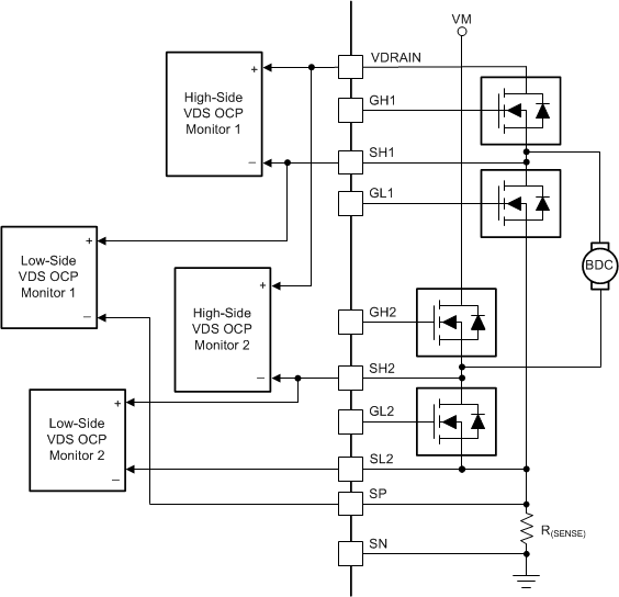
The gate-driver circuit monitors the VDS voltage of each external FET when it is driving current. When the voltage monitored is greater than the OCP threshold voltage (VDS(OCP)) after the OCP deglitch time has expired, an OCP condition is detected. The VDS(OCP) voltage can be adjusted by changing the resistor (RVDS) on the VDS pin of the DRV8702-Q1 device. The DRV8703-Q1 device provides VDS(OCP) voltage levels by setting the VDS register.
 Figure 7-13 VDS(OCP) Block Diagram
The VDS voltage on the high-side FET is measured across the VDRAIN to SHx pins. The low-side VDS monitor on half-bridge 1 measures the VDS voltage across the SH1 to SP pins. The low-side VDS monitor on half-bridge 2 measures the VDS voltage across the SH2 to SL2 pins. Ensure that the SP pin is always connected to the source of the low-side FET of half-bridge 1, even when the sense amplifier is not used.