ZHCSG57B March 2017 – December 2018 DRV8702D-Q1 , DRV8703D-Q1
PRODUCTION DATA.
- 1 特性
- 2 应用
- 3 说明
- 4 修订历史记录
- 5 Pin Configuration and Functions
- 6 Specifications
-
7 Detailed Description
- 7.1 Overview
- 7.2 Functional Block Diagram
- 7.3
Feature Description
- 7.3.1 Bridge Control
- 7.3.2 MODE Pin
- 7.3.3 nFAULT Pin
- 7.3.4 Current Regulation
- 7.3.5 Amplifier Output (SO)
- 7.3.6 PWM Motor Gate Drivers
- 7.3.7 IDRIVE Pin (DRV8702D-Q1 Only)
- 7.3.8 Dead Time
- 7.3.9 Propagation Delay
- 7.3.10 Overcurrent VDS Monitor
- 7.3.11 VDS Pin (DRV8702D-Q1 Only)
- 7.3.12 Charge Pump
- 7.3.13 Gate Drive Clamp
- 7.3.14
Protection Circuits
- 7.3.14.1 VM Undervoltage Lockout (UVLO2)
- 7.3.14.2 Logic Undervoltage (UVLO1)
- 7.3.14.3 VCP Undervoltage Lockout (CPUV)
- 7.3.14.4 Overcurrent Protection (OCP)
- 7.3.14.5 Gate Driver Fault (GDF)
- 7.3.14.6 Thermal Shutdown (TSD)
- 7.3.14.7 Watchdog Fault (WDFLT, DRV8703D-Q1 Only)
- 7.3.14.8 Reverse Supply Protection
- 7.3.15 Hardware Interface
- 7.4 Device Functional Modes
- 7.5 Programming
- 7.6 Register Maps
- 8 Application and Implementation
- 9 Power Supply Recommendations
- 10Layout
- 11器件和文档支持
- 12机械、封装和可订购信息
7.3.2 MODE Pin
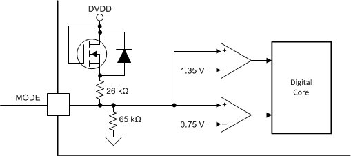
The MODE pin of the device determines the control interface and latches on power-up or when exiting sleep mode. Figure 32 shows an overview of the internal circuit of the MODE pin.
 Figure 32. MODE Pin Block Diagram
 Table 5 lists the different control interfaces that can be set via MODE pin at power-up or when exiting sleep mode.
Table 5. MODE Pin Configuration
| MODE | CONTROL INTERFACE |
|---|---|
| 1 | PWM control interface without current regulation |
| Hi-Z | PWM control interface with current regulation |
During the device power-up sequence, the DVDD pin is enabled first. Then the MODE pin latches. Finally the AVDD pin is enabled. For setting PWM control interface, TI does not recommended connecting the MODE pin to the AVDD pin. Instead the MODE pin should be connected to an external 5-V or 3.3-V supply or to the DVDD pin if not driven by an external microcontroller (MCU).