ZHCSG57B March 2017 – December 2018 DRV8702D-Q1 , DRV8703D-Q1
PRODUCTION DATA.
- 1 特性
- 2 应用
- 3 说明
- 4 修订历史记录
- 5 Pin Configuration and Functions
- 6 Specifications
-
7 Detailed Description
- 7.1 Overview
- 7.2 Functional Block Diagram
- 7.3
Feature Description
- 7.3.1 Bridge Control
- 7.3.2 MODE Pin
- 7.3.3 nFAULT Pin
- 7.3.4 Current Regulation
- 7.3.5 Amplifier Output (SO)
- 7.3.6 PWM Motor Gate Drivers
- 7.3.7 IDRIVE Pin (DRV8702D-Q1 Only)
- 7.3.8 Dead Time
- 7.3.9 Propagation Delay
- 7.3.10 Overcurrent VDS Monitor
- 7.3.11 VDS Pin (DRV8702D-Q1 Only)
- 7.3.12 Charge Pump
- 7.3.13 Gate Drive Clamp
- 7.3.14
Protection Circuits
- 7.3.14.1 VM Undervoltage Lockout (UVLO2)
- 7.3.14.2 Logic Undervoltage (UVLO1)
- 7.3.14.3 VCP Undervoltage Lockout (CPUV)
- 7.3.14.4 Overcurrent Protection (OCP)
- 7.3.14.5 Gate Driver Fault (GDF)
- 7.3.14.6 Thermal Shutdown (TSD)
- 7.3.14.7 Watchdog Fault (WDFLT, DRV8703D-Q1 Only)
- 7.3.14.8 Reverse Supply Protection
- 7.3.15 Hardware Interface
- 7.4 Device Functional Modes
- 7.5 Programming
- 7.6 Register Maps
- 8 Application and Implementation
- 9 Power Supply Recommendations
- 10Layout
- 11器件和文档支持
- 12机械、封装和可订购信息
7.3.6 PWM Motor Gate Drivers
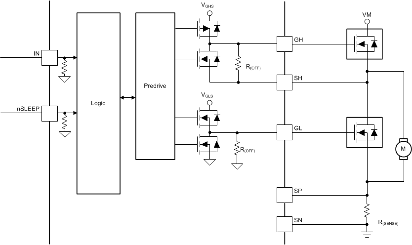
The DRV870xD-Q1 device has gate drivers for a single half-bridge with external NMOS FETs. Figure 37 shows a block diagram of the predrive circuitry.
 Figure 37. Predrive Block Diagram
 Gate drivers inside the DRV870xD-Q1 device directly drive N-Channel MOSFETs, which drive the motor current. The high-side gate drive is supplied by the charge pump, while an internal regulator generates the low-side gate drive.
The peak drive current of the gate drivers is adjustable through the IDRIVE pin for DRV8702D-Q1 device or the IDRIVE register for the DRV8703D-Q1 device. Peak source currents can be set to the values listed in the FET gate drivers section of the Electrical Characteristics table. The peak sink current is approximately two times the peak source current. Adjusting the peak current changes the output slew rate, which also depends on the FET input capacitance and gate charge.
Fast switching times can cause extra noise on the VM and GND pins. This additional noise can occur specifically because of a relatively slow reverse-recovery time of the low-side body diode, when the body diode conducts reverse-bias momentarily, similar to shoot-through. Slow switching times can cause excessive power dissipation because the external FETs have a longer turn on and turn off time.
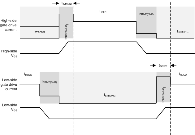
When changing the state of the output, the peak current (IDRIVE) is applied for a short period (t(DRIVE)), to charge the gate capacitance. After this time, a weak current source (IHOLD) is used to keep the gate at the desired state. When selecting the gate drive strength for a given external FET, the selected current must be high enough to charge fully and discharge the gate during t(DRIVE), or excessive power is dissipated in the FET.
During high-side turn on, the low-side gate is pulled low with a strong pulldown (ISTRONG). This pulldown prevents the low-side FET QGS from charging and keeps the FET off, even when fast switching occurs at the outputs.
The gate-driver circuits include enforcement of a dead time in analog circuitry, which prevents the high-side and low-side FETs from conducting at the same time. When the switching FETs are on, this handshaking prevents the high-side or low-side FET from turning on until the opposite FET turns off.
 Figure 38. Gate Driver Output to Control External FETs