ZHCSG08E October   2016  – January 2021 DRV8702-Q1 , DRV8703-Q1

PRODUCTION DATA  

  1. 特性
  2. 应用
  3. 说明
  4. Revision History
  5. Pin Configuration and Functions
    1.     Pin Functions
  6. Specifications
    1. 6.1 Absolute Maximum Ratings
    2. 6.2 ESD Ratings
    3. 6.3 Recommended Operating Conditions
    4. 6.4 Thermal Information
    5. 6.5 Electrical Characteristics
    6. 6.6 SPI Timing Requirements
    7. 6.7 Switching Characteristics
    8.     15
    9. 6.8 Typical Characteristics
  7. Detailed Description
    1. 7.1 Overview
    2. 7.2 Functional Block Diagram
    3. 7.3 Feature Description
      1. 7.3.1  Bridge Control
        1. 7.3.1.1 Logic Tables
      2. 7.3.2  MODE Pin
      3. 7.3.3  nFAULT Pin
      4. 7.3.4  Current Regulation
      5. 7.3.5  Amplifier Output (SO)
        1. 7.3.5.1 SO Sample and Hold Operation
      6. 7.3.6  PWM Motor Gate Drivers
        1. 7.3.6.1 Miller Charge (QGD)
      7. 7.3.7  IDRIVE Pin (DRV8702-Q1 Only)
      8. 7.3.8  Dead Time
      9. 7.3.9  Propagation Delay
      10. 7.3.10 Overcurrent VDS Monitor
      11. 7.3.11 VDS Pin (DRV8702-Q1 Only)
      12. 7.3.12 Charge Pump
      13. 7.3.13 Gate Drive Clamp
      14. 7.3.14 Protection Circuits
        1. 7.3.14.1 VM Undervoltage Lockout (UVLO2)
        2. 7.3.14.2 Logic Undervoltage (UVLO1)
        3. 7.3.14.3 VCP Undervoltage Lockout (CPUV)
        4. 7.3.14.4 Overcurrent Protection (OCP)
        5. 7.3.14.5 Gate Driver Fault (GDF)
        6. 7.3.14.6 Thermal Shutdown (TSD)
        7. 7.3.14.7 Watchdog Fault (WDFLT, DRV8703-Q1 Only)
        8. 7.3.14.8 Reverse Supply Protection
      15. 7.3.15 Hardware Interface
        1. 7.3.15.1 IDRIVE (6-level input)
        2. 7.3.15.2 VDS (6-Level Input)
    4. 7.4 Device Functional Modes
    5. 7.5 Programming
      1. 7.5.1 SPI Communication
        1. 7.5.1.1 Serial Peripheral Interface (SPI)
        2. 7.5.1.2 SPI Format
    6. 7.6 Register Maps
  8. Application and Implementation
    1. 8.1 Application Information
    2. 8.2 Typical Application
      1. 8.2.1 Design Requirements
      2. 8.2.2 Detailed Design Procedure
        1. 8.2.2.1 External FET Selection
        2. 8.2.2.2 IDRIVE Configuration
        3. 8.2.2.3 VDS Configuration
        4. 8.2.2.4 Current Chopping Configuration
      3. 8.2.3 Application Curves
  9. Power Supply Recommendations
    1. 9.1 Bulk Capacitance Sizing
  10. 10Layout
    1. 10.1 Layout Guidelines
    2. 10.2 Layout Example
  11. 11Device and Documentation Support
    1. 11.1 Documentation Support
      1. 11.1.1 Related Documentation
    2. 11.2 Related Links
    3. 11.3 接收文档更新通知
    4. 11.4 支持资源
    5. 11.5 Trademarks
    6. 11.6 静电放电警告
    7. 11.7 术语表
  12. 12Mechanical, Packaging, and Orderable Information

封装选项

请参考 PDF 数据表获取器件具体的封装图。

机械数据 (封装 | 引脚)
  • RHB|32
散热焊盘机械数据 (封装 | 引脚)
订购信息

Gate Drive Clamp

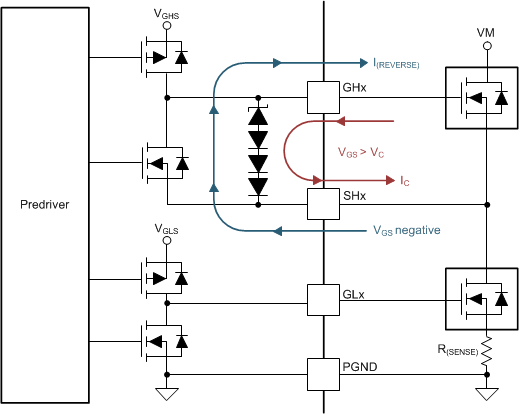
A clamping structure limits the gate-drive output voltage to the VC(GS) voltage to protect the power FETs from damage. The positive voltage clamp is realized using a series of diodes. The negative voltage clamp uses the body diodes of the internal predriver FET.
GUID-95074E9D-7CAA-4B29-BDE8-23753D285E08-low.gif Figure 7-16 Gate Drive Clamp