ZHCSEB6 October 2015 DRV8704
PRODUCTION DATA.
- 1 特性
- 2 应用
- 3 说明
- 4 修订历史记录
- 5 Pin Configuration and Functions
- 6 Specifications
-
7 Detailed Description
- 7.1 Overview
- 7.2 Functional Block Diagram
- 7.3 Feature Description
- 7.4 Device Functional Modes
- 7.5
Register Maps
- 7.5.1
Control Registers
- 7.5.1.1 CTRL Register (Address = 0x00h)
- 7.5.1.2 TORQUE Register (Address = 0x01h)
- 7.5.1.3 OFF Register (Address = 0x02h)
- 7.5.1.4 BLANK Register (Address = 0x03h)
- 7.5.1.5 DECAY Register (Address = 0x04h)
- 7.5.1.6 Reserved Register Address = 0x05h
- 7.5.1.7 DRIVE Register Address = 0x06h
- 7.5.1.8 STATUS Register (Address = 0x07h)
- 7.5.1
Control Registers
- 8 Application and Implementation
- 9 Power Supply Recommendations
- 10Layout
- 11器件和文档支持
- 12机械、封装和可订购信息
9 Power Supply Recommendations
The DRV8704 is designed to operate from an input voltage supply (VM) range between 8 and 52 V. A 0.01-μF ceramic capacitor rated for VM must be placed as close to the DRV8704 as possible. In addition, a bulk capacitor must be included on VM.
9.1 Bulk Capacitance
Having appropriate local bulk capacitance is an important factor in motor drive system design. It is generally beneficial to have more bulk capacitance, while the disadvantages are increased cost and physical size.
The amount of local capacitance needed depends on a variety of factors, including:
- The highest current required by the motor system
- The power supply’s capacitance and ability to source current
- The amount of parasitic inductance between the power supply and motor system
- The acceptable voltage ripple
- The type of motor used (brushed DC, brushless DC, stepper)
- The motor braking method
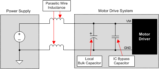
The inductance between the power supply and motor drive system will limit the rate current can change from the power supply. If the local bulk capacitance is too small, the system will respond to excessive current demands or dumps from the motor with a change in voltage. When adequate bulk capacitance is used, the motor voltage remains stable and high current can be quickly supplied.
The data sheet generally provides a recommended value, but system-level testing is required to determine the appropriate sized bulk capacitor.
 Figure 21. Example Setup of Motor Drive System With External Power Supply
The voltage rating for bulk capacitors should be higher than the operating voltage, to provide margin for cases when the motor transfers energy to the supply.