ZHCSEB6 October 2015 DRV8704
PRODUCTION DATA.
- 1 特性
- 2 应用
- 3 说明
- 4 修订历史记录
- 5 Pin Configuration and Functions
- 6 Specifications
-
7 Detailed Description
- 7.1 Overview
- 7.2 Functional Block Diagram
- 7.3 Feature Description
- 7.4 Device Functional Modes
- 7.5
Register Maps
- 7.5.1
Control Registers
- 7.5.1.1 CTRL Register (Address = 0x00h)
- 7.5.1.2 TORQUE Register (Address = 0x01h)
- 7.5.1.3 OFF Register (Address = 0x02h)
- 7.5.1.4 BLANK Register (Address = 0x03h)
- 7.5.1.5 DECAY Register (Address = 0x04h)
- 7.5.1.6 Reserved Register Address = 0x05h
- 7.5.1.7 DRIVE Register Address = 0x06h
- 7.5.1.8 STATUS Register (Address = 0x07h)
- 7.5.1
Control Registers
- 8 Application and Implementation
- 9 Power Supply Recommendations
- 10Layout
- 11器件和文档支持
- 12机械、封装和可订购信息
10 Layout
10.1 Layout Guidelines
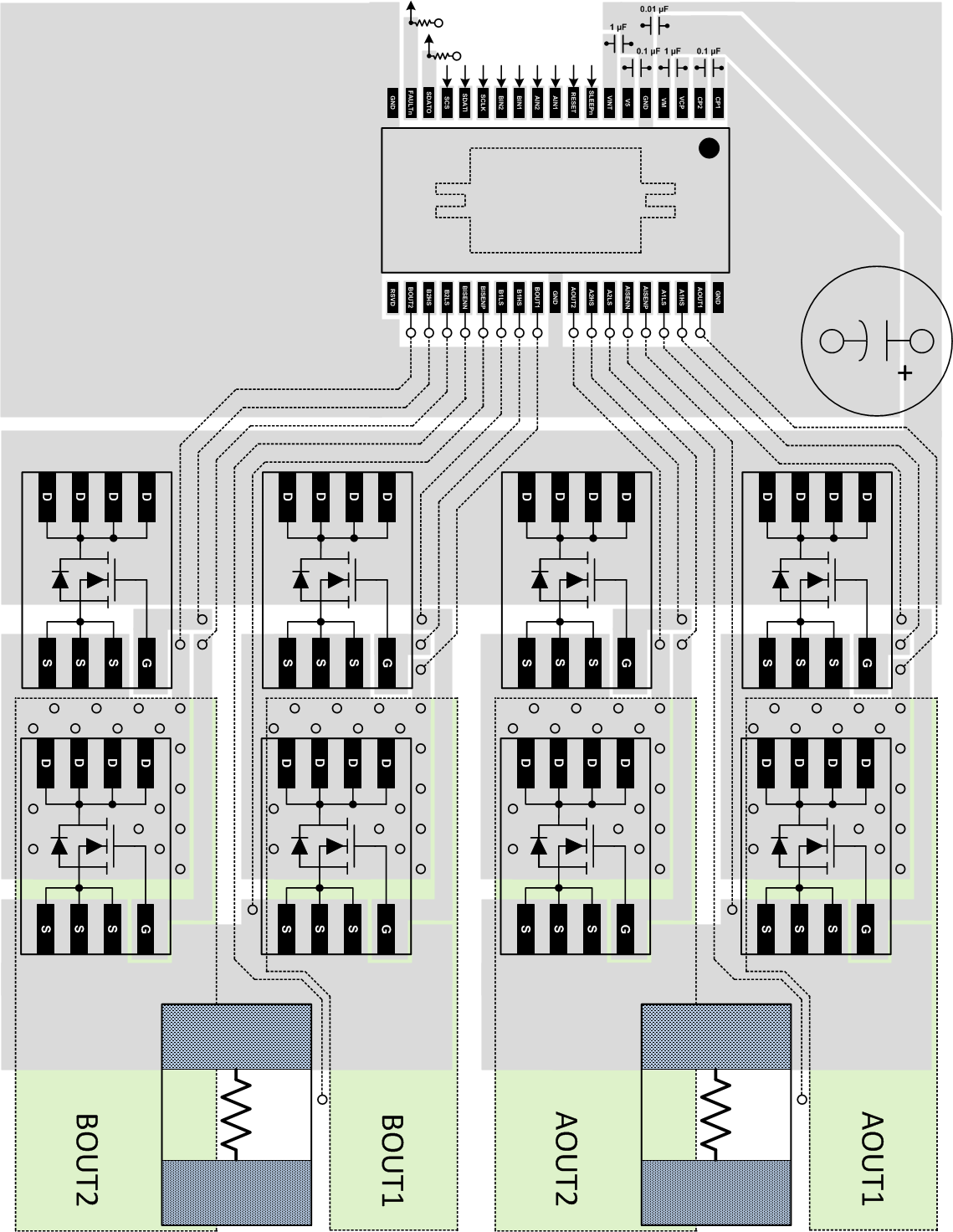
The VM terminal should be bypassed to GND using a low-ESR ceramic bypass capacitor with a recommended value of 0.01 μF rated for VM. This capacitor should be placed as close to the VM pin as possible with a thick trace or ground plane connection to the device GND pin.
The VM pin must be bypassed to ground using a bulk capacitor rated for VM. This component may be an electrolytic. The bulk capacitor should be placed to minimize the distance of the high-current path through the external FETs. The connecting metal trace widths should be as wide as possible, and numerous vias should be used when connecting PCB layers. These practices minimize inductance and allow the bulk capacitor to deliver high current.
A low-ESR ceramic capacitor must be placed in between the CPL and CPH pins. A value of 0.1 μF rated for VM is recommended. Place this component as close to the pins as possible.
A low-ESR ceramic capacitor must be placed in between the VM and VCP pins. A value of 1 μF rated for 16 V is recommended. Place this component as close to the pins as possible.
Bypass VINT to ground with a ceramic capacitor rated 6.3 V. Place this bypassing capacitor as close to the pin as possible.
Bypass V5 to ground with a ceramic capacitor rated 6.3 V. Place this bypassing capacitor as close to the pin as possible.
If desired, align the external NMOS FETs as shown on the next page to facilitate layout. Route the AOUT1, AOUT2, BOUT1, and BOUT2 nets to the motor windings.
Use separate traces to connect the xISENP and xISENN pins to the sense resistor terminals.
10.2 Layout Example
 Figure 22. Board Layout Example