ZHCSEB6 October 2015 DRV8704
PRODUCTION DATA.
- 1 特性
- 2 应用
- 3 说明
- 4 修订历史记录
- 5 Pin Configuration and Functions
- 6 Specifications
-
7 Detailed Description
- 7.1 Overview
- 7.2 Functional Block Diagram
- 7.3 Feature Description
- 7.4 Device Functional Modes
- 7.5
Register Maps
- 7.5.1
Control Registers
- 7.5.1.1 CTRL Register (Address = 0x00h)
- 7.5.1.2 TORQUE Register (Address = 0x01h)
- 7.5.1.3 OFF Register (Address = 0x02h)
- 7.5.1.4 BLANK Register (Address = 0x03h)
- 7.5.1.5 DECAY Register (Address = 0x04h)
- 7.5.1.6 Reserved Register Address = 0x05h
- 7.5.1.7 DRIVE Register Address = 0x06h
- 7.5.1.8 STATUS Register (Address = 0x07h)
- 7.5.1
Control Registers
- 8 Application and Implementation
- 9 Power Supply Recommendations
- 10Layout
- 11器件和文档支持
- 12机械、封装和可订购信息
8 Application and Implementation
NOTE
Information in the following applications sections is not part of the TI component specification, and TI does not warrant its accuracy or completeness. TI’s customers are responsible for determining suitability of components for their purposes. Customers should validate and test their design implementation to confirm system functionality.
8.1 Application Information
The DRV8704 is used in brushed DC motor control.
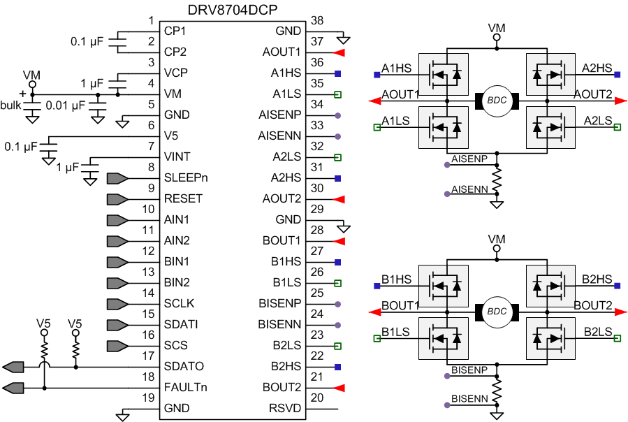
8.2 Typical Application
The following design procedure can be used to configure the DRV8704.
 Figure 18. Dual Brushed-DC Motor Control
8.2.1 Design Requirements
Table 12 shows design input parameters for system design.
Table 12. Design Parameters
| DESIGN PARAMETER | REFERENCE | EXAMPLE VALUE |
|---|---|---|
| Supply voltage | VM | 24 V |
| FET total gate charge (1) | Qg | 41 nC (typically) |
| FET gate-to-drain charge (1) | Qgd | 6.7 nC (typically) |
| Target FET gate rise time | RT | 20 to 100 ns |
| Motor winding resistance | RL | 400 mΩ |
| Motor winding inductance | LL | 258 μH |
| Target chopping current | ICHOP | 5.5 A |
8.2.2 Detailed Design Procedure
8.2.2.1 External FET Selection
The DRV8704 FET support is based on the charge pump capacity and output PWM frequency. For a quick calculation of FET driving capacity, use the following equations when drive and brake (slow decay) are the primary modes of operation:

where
- ƒPWM is the maximum desired PWM frequency to be applied to the DRV8704 inputs or the current chopping frequency, whichever is larger.
- IVCP is the charge pump capacity, which is 20 mA.
The factor of two arises because there are two H-bridges present.
The current chopping frequency is at most:

Example:
If a system uses a maximum PWM frequency of 40 kHz, then the DRV8704 will support Qg < 250 nC FETs.
If the application will require a forced fast decay (or alternating between drive and reverse drive), the maximum FET driving capacity is given by:

8.2.2.2 IDRIVE Configuration
IDRIVE is selected based on the gate charge of the FETs. The IDRIVEx and TDRIVEx registers need to be configured so that the FET gates are charged completely during TDRIVE. If IDRIVE is chosen to be too low for a given FET, or if TDRIVE is less than the intended rise time, then the FET may not turn on completely. TI suggests to adjust these values in-system with the required external FETs and motor to determine the best possible setting for any application.
For FETs with a known gate-to-drain charge Qgd and desired rise time RT, IDRIVE and TDRIVE can be selected based on:

Example:
If the gate-to-drain charge is 5.9 nC, and the desired rise time is around 20 to 100 ns:
IDRIVE1 = 6.7 nC / 20 ns = 335 mA
IDRIVE2 = 6.7 nC / 100 ns = 67 mA
Select IDRIVE between 67 and 335 mA.
We select IDRIVEP as 200-mA source and IDRIVEP as 400-mA sink.
We select TDRIVEN and TDRIVEP as 525 ns.
8.2.2.3 Current Chopping Configuration
The chopping current is set based on the sense resistor value, shunt amplifier gain set by the ISGAIN register, and the TORQUE register setting. The following is used to calculate the current:

Example:
If the desired chopping current is 5.5 A:
Set RSENSE = 100 mΩ.
Set ISGAIN to the 5 V/V setting.
The TORQUE register can be (decimal) 255.
8.2.2.4 Decay Modes
The DRV8704 supports several different decay modes: slow decay, fast decay, mixed decay, and automatic mixed decay. The current through the motor windings is regulated using an adjustable fixed-time-off scheme. This means that after any drive phase, when a motor winding current has hit the current chopping threshold (ITRIP), the DRV8704 will place the winding in one of the decay modes for TOFF. After TOFF, a new drive phase starts.
8.2.2.5 Sense Resistor
For optimal performance, it is important for the sense resistor to be:
- Surface-mount
- Low inductance
- Rated for high enough power
- Placed closely to the motor driver
The power dissipated by the sense resistor equals IRMS 2 × R. For example, if peak motor current is 3 A, RMS motor current is 2 A, and a 0.05-Ω sense resistor is used, the resistor will dissipate 2 A2 × 0.05 Ω = 0.2 W. The power quickly increases with higher current levels.
Resistors typically have a rated power within some ambient temperature range, along with a derated power curve for high ambient temperatures. When a PCB is shared with other components generating heat, margin should be added. It is always best to measure the actual sense resistor temperature in a final system, along with the power MOSFETs, as those are often the hottest components.
Because power resistors are larger and more expensive than standard resistors, it is common practice to use multiple standard resistors in parallel, between the sense node and ground. This distributes the current and heat dissipation.
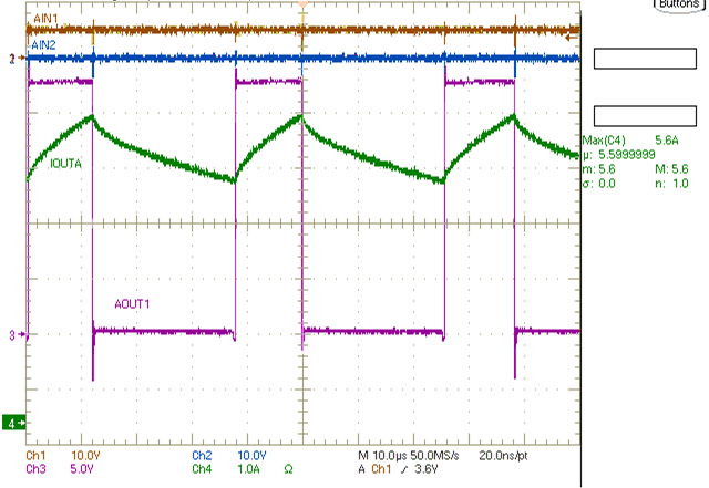
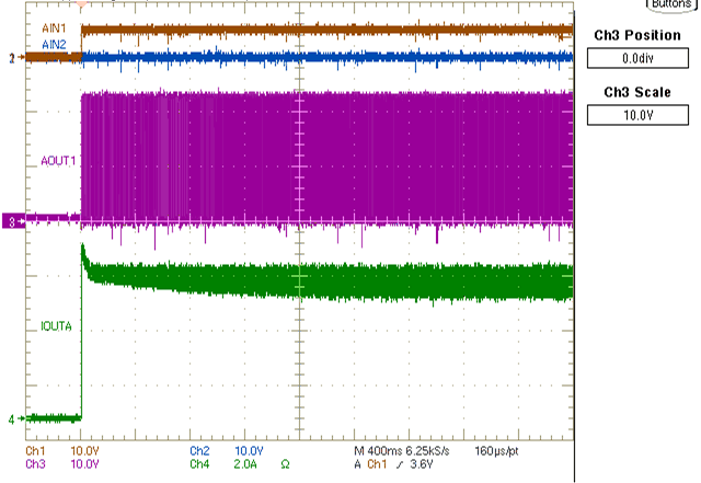
8.2.3 Application Curves

