ZHCSN08D August 2020 – April 2024 DRV8714-Q1 , DRV8718-Q1
PRODMIX
- 1
- 1 特性
- 2 应用
- 3 说明
- 4 Device Comparison Table
- 5 Pin Configuration and Functions
- 6 Specifications
-
7 Detailed Description
- 7.1 Overview
- 7.2 Functional Block Diagram
- 7.3
Feature Description
- 7.3.1 External Components
- 7.3.2 Device Interface Variants
- 7.3.3 Input PWM Control Modes
- 7.3.4 Smart Gate Driver
- 7.3.5 Tripler (Dual-Stage) Charge Pump
- 7.3.6 Wide Common-Mode Current Shunt Amplifiers
- 7.3.7 Pin Diagrams
- 7.3.8
Protection and Diagnostics
- 7.3.8.1 Gate Driver Disable (DRVOFF/nFLT and EN_DRV)
- 7.3.8.2 Low IQ Powered Off Braking (POB, BRAKE)
- 7.3.8.3 Fault Reset (CLR_FLT)
- 7.3.8.4 DVDD Logic Supply Power on Reset (DVDD_POR)
- 7.3.8.5 PVDD Supply Undervoltage Monitor (PVDD_UV)
- 7.3.8.6 PVDD Supply Overvoltage Monitor (PVDD_OV)
- 7.3.8.7 VCP Charge Pump Undervoltage Lockout (VCP_UV)
- 7.3.8.8 MOSFET VDS Overcurrent Protection (VDS_OCP)
- 7.3.8.9 Gate Driver Fault (VGS_GDF)
- 7.3.8.10 Thermal Warning (OTW)
- 7.3.8.11 Thermal Shutdown (OTSD)
- 7.3.8.12 Offline Short Circuit and Open Load Detection (OOL and OSC)
- 7.3.8.13 Watchdog Timer
- 7.3.8.14 Fault Detection and Response Summary Table
- 7.4 Device Functional Modes
- 7.5 Programming
- 8 Register Maps
- 9 Application Implementation
- 10Device Documentation and Support
- 11Revision History
- 12Mechanical, Packaging, and Orderable Information
封装选项
机械数据 (封装 | 引脚)
散热焊盘机械数据 (封装 | 引脚)
订购信息
7.3.6 Wide Common-Mode Current Shunt Amplifiers
The DRV871x-Q1 integrates two high-performance, wide common-mode, bidirectional, current-shunt amplifiers for current measurements using shunt resistors in the external half-bridges. Current measurements are commonly used to implement overcurrent protection, external torque control, or commutation with an external controller. Due to the high common-mode range of the shunt amplifier it can support low-side, high-side, or inline shunt configurations. The current shunt amplifiers include features such as programmable gain, unidirectional and bidirectional support, output blanking, and a dedicated voltage reference pin (AREF) to set a mid point bias voltage for the amplifier output. A simplified block diagram is shown in Figure 7-17. SPx should connect to the positive terminal of the shunt resistor and SNx should connect to the negative terminal of the shunt resistor. If the amplifiers are not utilized, the AREF, SNx, SPx inputs can be tied to AGND, AGND to PCB GND and the SOx outputs left floating.
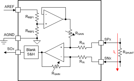 Figure 7-17 Amplifier
Simplified Block Diagram
Figure 7-17 Amplifier
Simplified Block DiagramA detailed block diagram is shown in Figure 7-18. The wide common mode amplifier is implemented with a two stage differential architecture. The 1st differential stage supports a wide common mode input, differential output, and has a fixed gain, G = 2. The 2nd differential stage supports a variable gain adjustment, G = 5, 10, 20, or 40. The total gain of the two stages will be G = 10, 20, 40, or 80.
The amplifier can also generate an output voltage bias through the AREF pin. The AREF pin goes to a divider network, a buffer, and then sets the output voltage bias for the differential amplifier. On SPI device variants, the gain is configured through the register setting CSA_GAIN and the reference division ratio through CSA_DIV. On H/W device variants, the reference division ratio is fixed to VAREF / 2. The gain is configured through the GAIN pin.
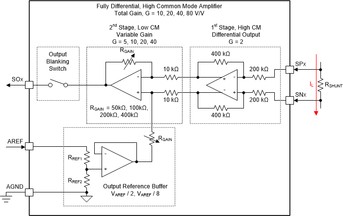 Figure 7-18 Amplifier
Detailed Block Diagram
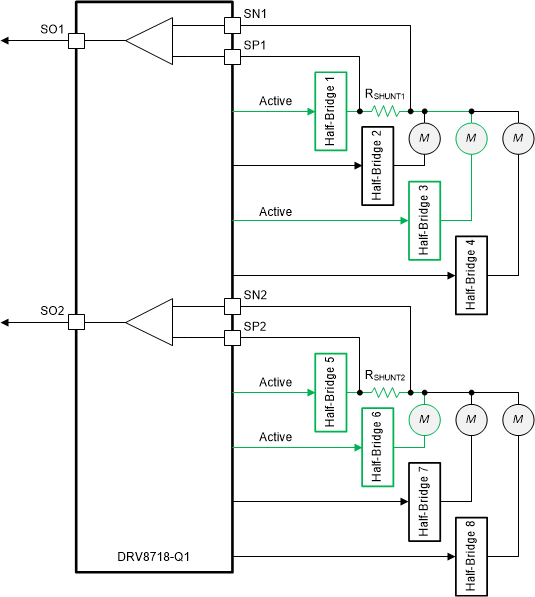 Figure 7-19 Shared Shunt
Resistor
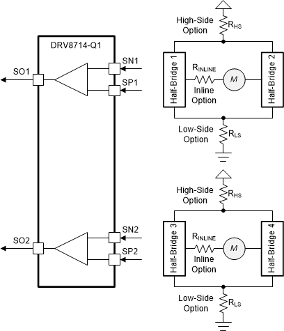 Figure 7-20 Individual H-Bridge Shunt
Resistor
Figure 7-20 Individual H-Bridge Shunt
ResistorThe DRV8718-Q1 inline shunt amplifier can be used to continuously sense motor current even in shared group or zone control configurations. The DRV8714-Q1 provides two shunt amplifiers for the four half-bridge gate drivers allowing for individual H-bridge current sensing if the system requires.
Lastly, the amplifier has an output blanking switch. This option is only available on SPI device variants. The output switch can be used to disconnect the amplifier output during PWM switching to reduce output noise (blanking). The blanking circuit can be set trigger on the active half-bridge (half-bridge 1-8) through the CSA_BLK_SEL_x register setting. The blanking period can be configured through the CSA_BLK_x register setting. If the gate drivers are transitioning between high-side and low-side FET turn on and turn off or vice versa, the blanking time will extend through the dead-time window to avoid amplifier signal noise if the output swings or noise couples during the dead-time period. An output hold up capacitor is recommended to stabilize the amplifier output when it is disconnected during blanking. Typically this capacitor should be after a series resistor in a RC filter configuration to limit direct capacitance seen directly at the amplifier output. An example of the blanking function is shown in Figure 7-21.
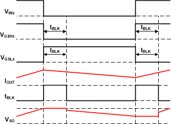 Figure 7-21 Amplifier Blanking
Example