ZHCSN08D August   2020  – April 2024 DRV8714-Q1 , DRV8718-Q1

PRODMIX  

  1.   1
  2. 特性
  3. 应用
  4. 说明
  5. Device Comparison Table
  6. Pin Configuration and Functions
    1. 5.1 VQFN (RVJ) 56-Pin Package and Pin Functions
    2. 5.2 VQFN (RHA) 40-Pin Package and Pin Functions
    3. 5.3 HTQFP (PHP) 48-Pin Package and Pin Functions
  7. Specifications
    1. 6.1 Absolute Maximum Ratings
    2. 6.2 ESD Ratings
    3. 6.3 Recommended Operating Conditions
    4. 6.4 Thermal Information
    5. 6.5 Electrical Characteristics
    6. 6.6 Timing Requirements
    7. 6.7 Timing Diagrams
    8. 6.8 Typical Characteristics
  8. Detailed Description
    1. 7.1 Overview
    2. 7.2 Functional Block Diagram
    3. 7.3 Feature Description
      1. 7.3.1 External Components
      2. 7.3.2 Device Interface Variants
        1. 7.3.2.1 Serial Peripheral Interface (SPI)
        2. 7.3.2.2 Hardware (H/W)
      3. 7.3.3 Input PWM Control Modes
        1. 7.3.3.1 Half-Bridge Control Scheme With Input PWM Mapping
          1. 7.3.3.1.1 DRV8718-Q1 Half-Bridge Control
          2. 7.3.3.1.2 DRV8714-Q1 Half-Bridge Control
        2. 7.3.3.2 H-Bridge Control
          1. 7.3.3.2.1 DRV8714-Q1 H-Bridge Control
        3. 7.3.3.3 Split HS and LS Solenoid Control
          1. 7.3.3.3.1 DRV8714-Q1 Split HS and LS Solenoid Control
      4. 7.3.4 Smart Gate Driver
        1. 7.3.4.1 Functional Block Diagram
        2. 7.3.4.2 Slew Rate Control (IDRIVE)
        3. 7.3.4.3 Gate Drive State Machine (TDRIVE)
        4. 7.3.4.4 Propagation Delay Reduction (PDR)
          1. 7.3.4.4.1 PDR Pre-Charge/Pre-Discharge Control Loop Operation Details
            1. 7.3.4.4.1.1 PDR Pre-Charge/Pre-Discharge Setup
          2. 7.3.4.4.2 PDR Post-Charge/Post-Discharge Control Loop Operation Details
            1. 7.3.4.4.2.1 PDR Post-Charge/Post-Discharge Setup
          3. 7.3.4.4.3 Detecting Drive and Freewheel MOSFET
        5. 7.3.4.5 Automatic Duty Cycle Compensation (DCC)
        6. 7.3.4.6 Closed Loop Slew Time Control (STC)
          1. 7.3.4.6.1 STC Control Loop Setup
      5. 7.3.5 Tripler (Dual-Stage) Charge Pump
      6. 7.3.6 Wide Common-Mode Current Shunt Amplifiers
      7. 7.3.7 Pin Diagrams
        1. 7.3.7.1 Logic Level Input Pin (INx/ENx, INx/PHx, nSLEEP, nSCS, SCLK, SDI)
        2. 7.3.7.2 Logic Level Push Pull Output (SDO)
        3. 7.3.7.3 Logic Level Multi-Function Pin (DRVOFF/nFLT)
        4. 7.3.7.4 Quad-Level Input (GAIN, MODE)
        5. 7.3.7.5 Six-Level Input (IDRIVE, VDS)
      8. 7.3.8 Protection and Diagnostics
        1. 7.3.8.1  Gate Driver Disable (DRVOFF/nFLT and EN_DRV)
        2. 7.3.8.2  Low IQ Powered Off Braking (POB, BRAKE)
        3. 7.3.8.3  Fault Reset (CLR_FLT)
        4. 7.3.8.4  DVDD Logic Supply Power on Reset (DVDD_POR)
        5. 7.3.8.5  PVDD Supply Undervoltage Monitor (PVDD_UV)
        6. 7.3.8.6  PVDD Supply Overvoltage Monitor (PVDD_OV)
        7. 7.3.8.7  VCP Charge Pump Undervoltage Lockout (VCP_UV)
        8. 7.3.8.8  MOSFET VDS Overcurrent Protection (VDS_OCP)
        9. 7.3.8.9  Gate Driver Fault (VGS_GDF)
        10. 7.3.8.10 Thermal Warning (OTW)
        11. 7.3.8.11 Thermal Shutdown (OTSD)
        12. 7.3.8.12 Offline Short Circuit and Open Load Detection (OOL and OSC)
        13. 7.3.8.13 Watchdog Timer
        14. 7.3.8.14 Fault Detection and Response Summary Table
    4. 7.4 Device Functional Modes
      1. 7.4.1 Inactive or Sleep State
      2. 7.4.2 Standby State
      3. 7.4.3 Operating State
    5. 7.5 Programming
      1. 7.5.1 SPI Interface
      2. 7.5.2 SPI Format
      3. 7.5.3 SPI Interface for Multiple Slaves
        1. 7.5.3.1 SPI Interface for Multiple Slaves in Daisy Chain
  9. Register Maps
    1. 8.1 DRV8718-Q1 Register Map
    2. 8.2 DRV8714-Q1 Register Map
    3. 8.3 DRV8718-Q1 Register Descriptions
      1. 8.3.1 DRV8718-Q1_STATUS Registers
      2. 8.3.2 DRV8718-Q1_CONTROL Registers
      3. 8.3.3 DRV8718-Q1_CONTROL_ADV Registers
      4. 8.3.4 DRV8718-Q1_STATUS_ADV Registers
    4. 8.4 DRV8714-Q1 Register Descriptions
      1. 8.4.1 DRV8714-Q1_STATUS Registers
      2. 8.4.2 DRV8714-Q1_CONTROL Registers
      3. 8.4.3 DRV8714-Q1_CONTROL_ADV Registers
      4. 8.4.4 DRV8714-Q1_STATUS_ADV Registers
  10. Application Implementation
    1. 9.1 Application Information
    2. 9.2 Typical Application
      1. 9.2.1 Design Requirements
      2. 9.2.2 Detailed Design Procedure
        1. 9.2.2.1 Gate Driver Configuration
          1. 9.2.2.1.1 VCP Load Calculation Example
          2. 9.2.2.1.2 IDRIVE Calculation Example
          3. 9.2.2.1.3 tDRIVE Calculation Example
          4. 9.2.2.1.4 Maximum PWM Switching Frequency
        2. 9.2.2.2 Current Shunt Amplifier Configuration
        3. 9.2.2.3 Power Dissipation
      3. 9.2.3 Application Curves
    3. 9.3 Initialization
    4. 9.4 Power Supply Recommendations
      1. 9.4.1 Bulk Capacitance Sizing
    5. 9.5 Layout
      1. 9.5.1 Layout Guidelines
      2. 9.5.2 Layout Example
  11. 10Device Documentation and Support
    1. 10.1 Documentation Support
      1. 10.1.1 Related Documents
    2. 10.2 接收文档更新通知
    3. 10.3 支持资源
    4. 10.4 Trademarks
    5. 10.5 静电放电警告
    6. 10.6 术语表
  12. 11Revision History
  13. 12Mechanical, Packaging, and Orderable Information
    1. 12.1 Package Option Addendum

封装选项

机械数据 (封装 | 引脚)
散热焊盘机械数据 (封装 | 引脚)
订购信息

SPI Interface for Multiple Slaves

Multiple DRV871x-Q1 devices can be connected to the master controller with and without the daisy chain. For connecting a 'n' number of DRV871x-Q1 to a master controller without using a daisy chain, 'n' number of I/O resources from master controller has to utilized for nSCS pins as shown Figure 7-32. Whereas, if the daisy chain configuration is used, then a single nSCS line can be used for connecting multiple DRV871x-Q1 devices. Figure 7-33
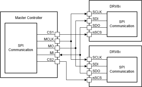
DRV8714-Q1 DRV8718-Q1 SPI Operation Without Daisy ChainFigure 7-32 SPI Operation Without Daisy Chain
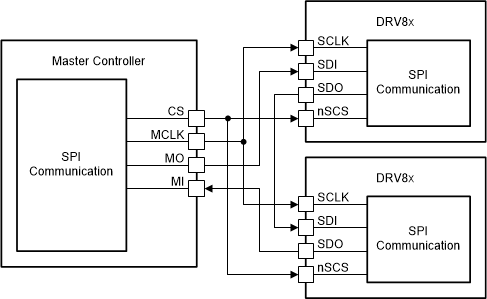
DRV8714-Q1 DRV8718-Q1 SPI Operation With Daisy ChainFigure 7-33 SPI Operation With Daisy Chain