ZHCSN08D August   2020  – April 2024 DRV8714-Q1 , DRV8718-Q1

PRODMIX  

  1.   1
  2. 特性
  3. 应用
  4. 说明
  5. Device Comparison Table
  6. Pin Configuration and Functions
    1. 5.1 VQFN (RVJ) 56-Pin Package and Pin Functions
    2. 5.2 VQFN (RHA) 40-Pin Package and Pin Functions
    3. 5.3 HTQFP (PHP) 48-Pin Package and Pin Functions
  7. Specifications
    1. 6.1 Absolute Maximum Ratings
    2. 6.2 ESD Ratings
    3. 6.3 Recommended Operating Conditions
    4. 6.4 Thermal Information
    5. 6.5 Electrical Characteristics
    6. 6.6 Timing Requirements
    7. 6.7 Timing Diagrams
    8. 6.8 Typical Characteristics
  8. Detailed Description
    1. 7.1 Overview
    2. 7.2 Functional Block Diagram
    3. 7.3 Feature Description
      1. 7.3.1 External Components
      2. 7.3.2 Device Interface Variants
        1. 7.3.2.1 Serial Peripheral Interface (SPI)
        2. 7.3.2.2 Hardware (H/W)
      3. 7.3.3 Input PWM Control Modes
        1. 7.3.3.1 Half-Bridge Control Scheme With Input PWM Mapping
          1. 7.3.3.1.1 DRV8718-Q1 Half-Bridge Control
          2. 7.3.3.1.2 DRV8714-Q1 Half-Bridge Control
        2. 7.3.3.2 H-Bridge Control
          1. 7.3.3.2.1 DRV8714-Q1 H-Bridge Control
        3. 7.3.3.3 Split HS and LS Solenoid Control
          1. 7.3.3.3.1 DRV8714-Q1 Split HS and LS Solenoid Control
      4. 7.3.4 Smart Gate Driver
        1. 7.3.4.1 Functional Block Diagram
        2. 7.3.4.2 Slew Rate Control (IDRIVE)
        3. 7.3.4.3 Gate Drive State Machine (TDRIVE)
        4. 7.3.4.4 Propagation Delay Reduction (PDR)
          1. 7.3.4.4.1 PDR Pre-Charge/Pre-Discharge Control Loop Operation Details
            1. 7.3.4.4.1.1 PDR Pre-Charge/Pre-Discharge Setup
          2. 7.3.4.4.2 PDR Post-Charge/Post-Discharge Control Loop Operation Details
            1. 7.3.4.4.2.1 PDR Post-Charge/Post-Discharge Setup
          3. 7.3.4.4.3 Detecting Drive and Freewheel MOSFET
        5. 7.3.4.5 Automatic Duty Cycle Compensation (DCC)
        6. 7.3.4.6 Closed Loop Slew Time Control (STC)
          1. 7.3.4.6.1 STC Control Loop Setup
      5. 7.3.5 Tripler (Dual-Stage) Charge Pump
      6. 7.3.6 Wide Common-Mode Current Shunt Amplifiers
      7. 7.3.7 Pin Diagrams
        1. 7.3.7.1 Logic Level Input Pin (INx/ENx, INx/PHx, nSLEEP, nSCS, SCLK, SDI)
        2. 7.3.7.2 Logic Level Push Pull Output (SDO)
        3. 7.3.7.3 Logic Level Multi-Function Pin (DRVOFF/nFLT)
        4. 7.3.7.4 Quad-Level Input (GAIN, MODE)
        5. 7.3.7.5 Six-Level Input (IDRIVE, VDS)
      8. 7.3.8 Protection and Diagnostics
        1. 7.3.8.1  Gate Driver Disable (DRVOFF/nFLT and EN_DRV)
        2. 7.3.8.2  Low IQ Powered Off Braking (POB, BRAKE)
        3. 7.3.8.3  Fault Reset (CLR_FLT)
        4. 7.3.8.4  DVDD Logic Supply Power on Reset (DVDD_POR)
        5. 7.3.8.5  PVDD Supply Undervoltage Monitor (PVDD_UV)
        6. 7.3.8.6  PVDD Supply Overvoltage Monitor (PVDD_OV)
        7. 7.3.8.7  VCP Charge Pump Undervoltage Lockout (VCP_UV)
        8. 7.3.8.8  MOSFET VDS Overcurrent Protection (VDS_OCP)
        9. 7.3.8.9  Gate Driver Fault (VGS_GDF)
        10. 7.3.8.10 Thermal Warning (OTW)
        11. 7.3.8.11 Thermal Shutdown (OTSD)
        12. 7.3.8.12 Offline Short Circuit and Open Load Detection (OOL and OSC)
        13. 7.3.8.13 Watchdog Timer
        14. 7.3.8.14 Fault Detection and Response Summary Table
    4. 7.4 Device Functional Modes
      1. 7.4.1 Inactive or Sleep State
      2. 7.4.2 Standby State
      3. 7.4.3 Operating State
    5. 7.5 Programming
      1. 7.5.1 SPI Interface
      2. 7.5.2 SPI Format
      3. 7.5.3 SPI Interface for Multiple Slaves
        1. 7.5.3.1 SPI Interface for Multiple Slaves in Daisy Chain
  9. Register Maps
    1. 8.1 DRV8718-Q1 Register Map
    2. 8.2 DRV8714-Q1 Register Map
    3. 8.3 DRV8718-Q1 Register Descriptions
      1. 8.3.1 DRV8718-Q1_STATUS Registers
      2. 8.3.2 DRV8718-Q1_CONTROL Registers
      3. 8.3.3 DRV8718-Q1_CONTROL_ADV Registers
      4. 8.3.4 DRV8718-Q1_STATUS_ADV Registers
    4. 8.4 DRV8714-Q1 Register Descriptions
      1. 8.4.1 DRV8714-Q1_STATUS Registers
      2. 8.4.2 DRV8714-Q1_CONTROL Registers
      3. 8.4.3 DRV8714-Q1_CONTROL_ADV Registers
      4. 8.4.4 DRV8714-Q1_STATUS_ADV Registers
  10. Application Implementation
    1. 9.1 Application Information
    2. 9.2 Typical Application
      1. 9.2.1 Design Requirements
      2. 9.2.2 Detailed Design Procedure
        1. 9.2.2.1 Gate Driver Configuration
          1. 9.2.2.1.1 VCP Load Calculation Example
          2. 9.2.2.1.2 IDRIVE Calculation Example
          3. 9.2.2.1.3 tDRIVE Calculation Example
          4. 9.2.2.1.4 Maximum PWM Switching Frequency
        2. 9.2.2.2 Current Shunt Amplifier Configuration
        3. 9.2.2.3 Power Dissipation
      3. 9.2.3 Application Curves
    3. 9.3 Initialization
    4. 9.4 Power Supply Recommendations
      1. 9.4.1 Bulk Capacitance Sizing
    5. 9.5 Layout
      1. 9.5.1 Layout Guidelines
      2. 9.5.2 Layout Example
  11. 10Device Documentation and Support
    1. 10.1 Documentation Support
      1. 10.1.1 Related Documents
    2. 10.2 接收文档更新通知
    3. 10.3 支持资源
    4. 10.4 Trademarks
    5. 10.5 静电放电警告
    6. 10.6 术语表
  12. 11Revision History
  13. 12Mechanical, Packaging, and Orderable Information
    1. 12.1 Package Option Addendum

封装选项

机械数据 (封装 | 引脚)
散热焊盘机械数据 (封装 | 引脚)
订购信息

SPI Interface

An SPI bus is used to set device configurations, operating parameters, and read out diagnostic information on the DRV871x-Q1 devices. The SPI operates in slave mode and connects to a master controller. The SPI input data (SDI) word consists of a 16 bit word, with an 8 bit command and 8 bits of data. The SPI output data (SDO) word consists of the fault status indication bits and then the register data being accessed for read commands or null for write commands. The data sequence between the MCU and the SPI slave driver is shown in Figure 7-30.

DRV8714-Q1 DRV8718-Q1 SPI Data FrameFigure 7-30 SPI Data Frame

A valid frame must meet the following conditions:

  • The SCLK pin should be low when the nSCS pin transitions from high to low and from low to high.
  • The nSCS pin should be pulled high between words.
  • When the nSCS pin is pulled high, any signals at the SCLK and SDI pins are ignored and the SDO pin is placed in the Hi-Z state.
  • Data is captured on the falling edge of SCLK and data is propagated on the rising edge of SCLK.
  • The most significant bit (MSB) is shifted in and out first.
  • A full 16 SCLK cycles must occur for transaction to be valid.
  • If the data word sent to the SDI pin is less than or more than 16 bits, a frame error (SCLK_FLT) occurs and the data word is ignored.
  • For a write command, the existing data in the register being written to is shifted out on the SDO pin follow the 8 bit command data.
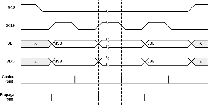
DRV8714-Q1 DRV8718-Q1 SPI Slave Timing Diagram Figure 7-31 SPI Slave Timing Diagram